


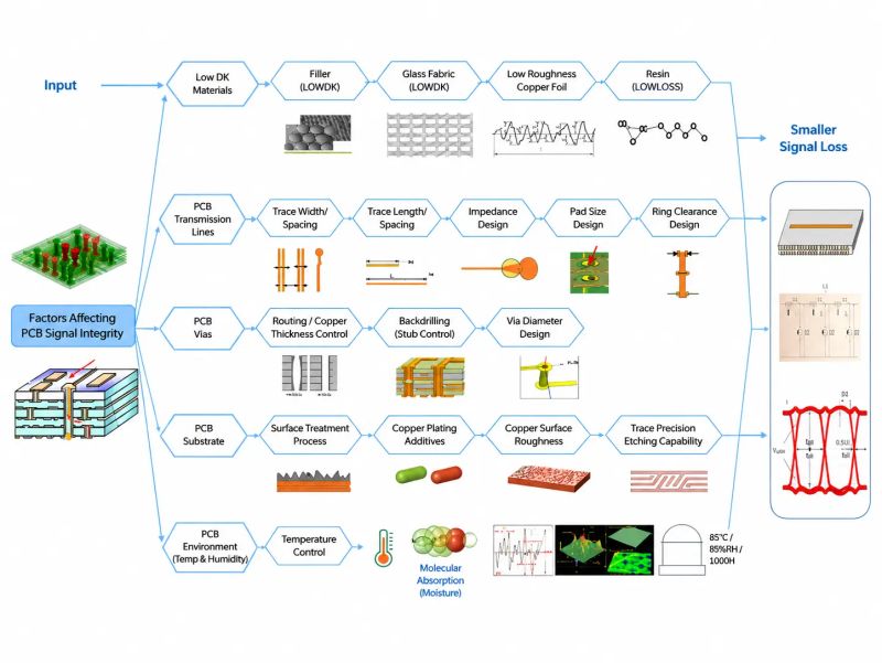
As digital interfaces move toward higher data rates and RF circuits operate at higher frequencies, PCB traces can no longer be treated as simple electrical connections.
Every transmission path is affected by the dielectric material, copper structure, trace geometry, vias, surface treatment, manufacturing accuracy, and operating environment. If these factors are not controlled, the PCB may experience excessive insertion loss, reflections, impedance discontinuities, crosstalk, jitter, and eye-diagram degradation.
This guide explains the major factors affecting PCB signal integrity and shows how engineers can reduce signal loss from material selection through PCB fabrication and environmental control.
Table of Contents
- Understand PCB Signal Loss and Signal Integrity
- Select Low-Loss PCB Materials
- Optimize PCB Transmission-Line Geometry
- Control Via Structures and Layer Transitions
- Improve PCB Substrate and Copper Quality
- Control Temperature and Moisture
- Verify Signal Integrity Before Manufacturing
- Test and Optimize the Finished PCB
- FAQ About PCB Signal Integrity
- Conclusion
Key Factors Affecting PCB Signal Integrity
The primary factors can be divided into five groups:
| 类别 | Main Factors |
|---|---|
| PCB materials | Dielectric constant, dissipation factor, resin system, glass fabric and copper roughness |
| Transmission lines | Trace width, spacing, length, impedance, pad geometry and plane clearance |
| Via structures | Via diameter, stub length, copper thickness, routing method and backdrilling |
| Manufacturing | Surface finish, plating additives, copper roughness and etching accuracy |
| Environment | Temperature, humidity and moisture absorption |
These factors interact with one another. Changing the dielectric material, for example, may require a new trace width to maintain the target impedance.
Step 1: Understand PCB Signal Loss and Signal Integrity
What Is PCB Signal Integrity?
Signal integrity describes the ability of an electrical signal to travel from its transmitter to its receiver while maintaining an acceptable waveform, timing margin and voltage level.
A signal-integrity problem may appear as:
- Excessive overshoot or undershoot
- Signal reflections
- Crosstalk between adjacent traces
- Reduced eye opening
- Timing jitter
- Attenuation at the receiver
- Unstable high-speed communication
- Increased bit-error rate
At low frequencies, a PCB trace may behave almost like an ideal wire. At higher frequencies, however, the trace becomes a transmission line whose electrical properties depend on the entire PCB stackup.
Where Does Signal Loss Come From?
PCB signal attenuation generally comes from several mechanisms:
Dielectric Loss
Part of the electromagnetic energy is absorbed by the PCB dielectric and converted into heat.
Conductor Loss
Current flowing through copper experiences resistance. At high frequencies, skin effect concentrates the current near the copper surface, making surface condition increasingly important.
Reflection Loss
When the signal encounters an impedance discontinuity, part of its energy is reflected toward the source.
Radiation and Coupling Loss
Poor return-path design, excessive loop area and nearby traces can cause electromagnetic radiation or coupling.
The objective of signal-integrity design is not to eliminate every loss mechanism, but to keep the total channel loss within the transmitter and receiver budgets.
Step 2: Select Low-Loss PCB Materials
Material selection determines the basic electrical behavior of a high-speed PCB.
Choose a Low-Dk Material
The dielectric constant, commonly written as Dk 或者 εr, affects signal propagation velocity and transmission-line impedance.
A lower and more stable Dk can help:
- Reduce propagation delay
- Improve impedance predictability
- Support wider traces for a given impedance
- Reduce variation between different production batches
- Improve phase consistency in RF circuits
However, the lowest available Dk is not automatically the best choice. Cost, mechanical strength, thermal performance and fabrication capability must also be considered.
Choose a Low-Df Material
The dissipation factor, or Df, represents dielectric energy loss.
For long high-speed channels, high-frequency RF circuits, SerDes links and data-center hardware, a lower Df generally produces lower insertion loss.
Material selection should consider the Df value at the actual operating frequency rather than relying only on a low-frequency datasheet value.
Evaluate the Resin System and Filler
The resin formulation influences:
- Dielectric loss
- Moisture resistance
- Thermal stability
- Glass-transition temperature
- Z-axis expansion
- Long-term material reliability
Ceramic or mineral fillers may be added to improve dimensional, thermal or dielectric characteristics. However, filler size and distribution must remain sufficiently uniform to prevent local dielectric variation.
Consider the Glass-Fabric Style
Woven glass fabric creates regions containing different proportions of resin and glass.
Because glass and resin have different dielectric constants, a trace passing over an uneven weave pattern may experience localized impedance or propagation-delay variation. This is commonly known as the glass-weave effect.
Possible mitigation methods include:
- Selecting spread-glass or flatter-weave materials
- Routing critical traces at a slight angle to the weave
- Using broader traces where the design allows
- Working with the PCB manufacturer to choose an appropriate laminate construction
Use Low-Profile Copper Foil
Copper roughness increases the effective path traveled by high-frequency current.
For loss-sensitive designs, consider:
- Very-low-profile copper
- Hyper-very-low-profile copper
- Reverse-treated copper
- Smooth copper systems approved for high-speed laminates
The selected foil must still provide sufficient bonding strength between copper and dielectric material.
Material Selection Checklist
| 范围 | Recommended Design Goal |
|---|---|
| Dk | Low, stable and well characterized |
| Df | Appropriate for the target frequency and channel length |
| Glass fabric | Spread or low-weave-effect construction |
| Copper foil | Low-profile copper for loss-sensitive channels |
| Resin | Low moisture absorption and stable thermal performance |
| Supplier data | Frequency-dependent and construction-specific values |
Step 3: Optimize PCB Transmission-Line Geometry
Once the laminate and stackup are selected, the next step is to design the transmission lines.
Calculate Trace Width and Spacing
Trace width, dielectric thickness, copper thickness and reference-plane position determine the characteristic impedance.
Common impedance targets include:
- 50 Ω single-ended
- 90 Ω differential
- 100 Ω differential
- Application-specific RF impedances
Trace spacing also affects differential coupling and crosstalk.
Critical trace dimensions should be calculated using the actual stackup supplied by the PCB manufacturer rather than a generic online stackup.
Keep Critical Traces as Short as Practical
Longer traces generally introduce more:
- Conductor loss
- Dielectric loss
- Propagation delay
- Crosstalk exposure
- Phase mismatch risk
Component placement should therefore be optimized before detailed routing begins.
Place high-speed transmitters, receivers, connectors and memory devices to minimize unnecessary channel length.
Maintain Continuous Reference Planes
A high-speed signal does not travel through the trace alone. Its return current flows through the adjacent reference plane.
Avoid routing critical traces across:
- Plane splits
- Large voids
- Isolated copper regions
- Unreferenced layer transitions
- Cutouts beneath connectors
A discontinuous return path increases loop area and may create radiation, crosstalk and impedance variation.
Control Impedance Throughout the Channel
A nominally controlled-impedance trace may still contain local discontinuities caused by:
- Pads
- Test points
- Connectors
- Vias
- Layer transitions
- Neck-down regions
- Copper-pour clearance
- Component packages
The complete signal path should be treated as a channel rather than evaluating only its straight trace sections.
Optimize Pad Size
Oversized pads add parasitic capacitance and can reduce local impedance.
For high-speed components, pad dimensions should be based on:
- Component land-pattern requirements
- Assembly tolerances
- Solder-joint reliability
- Escape-routing requirements
- Signal-integrity simulation results
Reducing unnecessary pad area can improve the electrical transition, but pads must remain manufacturable.
Manage Plane Clearance Around Pads and Vias
Large anti-pads reduce parasitic capacitance but may disturb the reference plane. Small anti-pads preserve the plane but increase capacitive loading.
The optimum clearance depends on:
- Layer count
- Via type
- Target impedance
- Drill diameter
- Pad diameter
- Reference-plane configuration
For sensitive SerDes or RF channels, anti-pad geometry should be included in three-dimensional electromagnetic simulation.
Step 4: Control Via Structures and Layer Transitions
Vias are among the most common sources of impedance discontinuity in multilayer PCBs.
Select an Appropriate Via Diameter
Via diameter affects:
- Parasitic inductance
- Parasitic capacitance
- Current capacity
- Drilling tolerance
- Aspect ratio
- Available routing space
A smaller via may reduce pad area and capacitive loading, but it can also increase fabrication complexity and cost.
The correct geometry should be selected according to both electrical and manufacturing requirements.
Minimize Unused Via Stubs
When a through-hole via connects only a few layers, the unused section becomes a stub.
At sufficiently high frequencies, the stub may behave as a resonant structure and cause insertion-loss notches or reflections.
Common solutions include:
- Blind vias
- Buried vias
- Microvias
- Backdrilling
- Optimized layer assignments
Use Backdrilling for Long High-Speed Channels
Backdrilling removes the unused portion of a plated through-hole after PCB fabrication.
It is commonly used for:
- High-speed connectors
- Backplanes
- Server boards
- Telecom equipment
- FPGA transceiver channels
- Long SerDes links
Important backdrilling parameters include:
- Remaining stub length
- Drill-to-copper clearance
- Backdrill diameter
- Target layer
- Registration tolerance
The remaining stub should be defined according to the channel frequency and the PCB manufacturer’s drilling capability.
Add Return Vias Near Signal-Layer Transitions
When a signal changes reference planes, its return current also needs a path between those planes.
Place ground stitching vias close to critical signal vias, especially when:
- A differential pair changes layers
- A signal moves between different reference planes
- The board contains multiple ground regions
- The return path must pass through decoupling capacitors
For differential pairs, via structures should remain symmetrical to reduce mode conversion and skew.
Via Design Checklist
| 物品 | Design Consideration |
|---|---|
| Drill diameter | Electrical performance and manufacturability |
| Pad diameter | Annular-ring requirement and parasitic capacitance |
| Anti-pad | Reference-plane integrity and impedance control |
| Stub length | Resonance and insertion-loss impact |
| Return vias | Continuous return-current path |
| Pair symmetry | Differential skew and common-mode conversion |
Step 5: Improve PCB Substrate and Copper Quality
Signal integrity is influenced not only by the layout but also by the PCB manufacturing process.
Select an Appropriate Surface Finish
Common PCB surface finishes include:
- HASL
- Lead-free HASL
- ENIG
- ENEPIG
- Immersion silver
- Immersion tin
- OSP
The surface finish affects solderability, pad flatness, storage life, assembly compatibility and the final conductor surface.
For fine-pitch components and high-density assembly, a flatter surface finish is normally preferred.
For RF conductors, the final metal structure should also be reviewed because additional metallic layers can influence conductor loss.
Control Copper Plating
Copper-plating thickness affects via reliability, trace dimensions and conductor geometry.
Variation in plating can change:
- Finished copper thickness
- Trace impedance
- Via-barrel dimensions
- Pad geometry
- Conductor resistance
The fabrication drawing should specify the required finished copper thickness instead of relying only on the starting copper weight.
Review Plating Additives and Process Chemistry
PCB plating processes use additives to control deposition rate, leveling and surface structure.
For standard digital boards, these effects may be relatively small. For high-frequency or low-loss designs, however, the final copper morphology and plated structure may need tighter process control.
Material and process selections should therefore be discussed with the PCB manufacturer before production.
Specify Copper Surface Roughness
The laminate datasheet may describe the copper foil, but the final board may contain multiple copper surfaces created by different processes.
Review:
- Base copper type
- Treated side of the foil
- Plated copper condition
- Inner-layer treatment
- Bond-enhancement process
- Roughness values used in simulation
The roughness model used in signal-integrity simulation should correspond as closely as possible to the actual manufacturing process.
Ensure Accurate Trace Etching
Etching variation can change trace width and cross-sectional shape.
Potential problems include:
- Over-etching
- Under-etching
- Trapezoidal trace profiles
- Uneven differential-pair widths
- Local spacing variation
- Reduced conductor thickness
High-speed boards should therefore include explicit controlled-impedance requirements and impedance test coupons.
Step 6: Control Temperature and Moisture
Environmental conditions can change the electrical properties of the PCB.
Understand Temperature Effects
Temperature can influence:
- Dielectric constant
- Dissipation factor
- Copper resistance
- Resin expansion
- Via stress
- Component timing
- Connector performance
A design that passes at room temperature may behave differently at the upper or lower limit of its operating range.
Applications such as automotive electronics, industrial controls and outdoor telecom equipment should be validated over the full specified temperature range.
Reduce Moisture Absorption
Moisture absorbed by the laminate can alter its dielectric properties and increase loss.
Moisture can also contribute to:
- Delamination
- Conductive anodic filament risk
- Leakage-current growth
- Corrosion
- Assembly defects during reflow
Choose materials with appropriate moisture resistance and follow proper storage and baking procedures before assembly when required.
Apply Environmental Protection Where Necessary
Boards operating in humid, contaminated or condensing environments may require:
- Conformal coating
- Protective enclosure
- Edge sealing
- Controlled storage
- Humidity testing
- Ionic-contamination control
Coatings must be selected carefully because they can also alter RF behavior around exposed transmission lines and antennas.
Step 7: Verify Signal Integrity Before Manufacturing
Simulation helps identify problems before committing the design to fabrication.
Build an Accurate Stackup Model
The simulation model should include:
- Finished dielectric thickness
- Copper thickness
- Dk and Df at the target frequency
- Copper roughness
- Solder mask where relevant
- Trace cross-sectional shape
- Reference-plane location
- Differential-pair spacing
Generic material values may produce misleading results.
Run Pre-Layout Analysis
Pre-layout analysis can help determine:
- Suitable layer assignments
- Trace width and spacing
- Maximum channel length
- Acceptable via count
- Termination strategy
- Material requirements
This stage is especially important when comparing a standard FR-4 construction with a low-loss laminate.
Run Post-Layout Channel Analysis
After routing is complete, extract the actual channel and evaluate:
- Insertion loss
- Return loss
- Impedance profile
- Crosstalk
- Differential skew
- Mode conversion
- Eye diagram
- Timing margin
For complex connectors and via structures, use an S-parameter or three-dimensional electromagnetic model.
Review the Complete Signal Path
The analysis should include more than the PCB traces.
A practical channel may contain:
- Package breakout
- BGA vias
- PCB traces
- AC-coupling capacitors
- Test pads
- Connectors
- Cables
- Receiver package
Optimizing one section while ignoring the others may not improve the complete channel.
Step 8: Test and Optimize the Finished PCB
Measure Controlled Impedance
A time-domain reflectometer can be used to examine impedance variation along a test coupon or signal channel.
The measurement can reveal:
- Trace-impedance deviation
- Via discontinuities
- Connector transitions
- Open or short defects
- Unexpected geometry changes
PCB manufacturers commonly use impedance coupons to verify that the fabricated board meets the specified tolerance.
Measure Insertion Loss
Insertion loss is typically evaluated using a vector network analyzer and suitable test fixtures.
The result helps confirm whether:
- Material loss matches expectations
- Copper roughness is acceptable
- Via stubs create resonances
- Connectors introduce excessive attenuation
- Manufacturing variation affects channel performance
Fixture de-embedding may be necessary to separate the PCB channel from the measurement interface.
Inspect the Eye Diagram
An eye diagram provides a direct view of received signal quality.
Important characteristics include:
- Eye height
- Eye width
- Jitter
- Noise
- Crossing symmetry
- Overshoot
- Data-dependent distortion
A reduced eye opening does not identify a single root cause by itself, but it indicates that the complete channel is consuming too much signal margin.
Compare Simulation and Measurement
If measurement differs significantly from simulation, review:
- Actual PCB stackup
- Fabricated trace dimensions
- Copper roughness assumptions
- Connector and fixture models
- Material Dk and Df values
- Via-stub dimensions
- Test-equipment calibration
- Temperature and humidity conditions
Correlation between simulation and measurement improves the accuracy of future PCB designs.
Practical PCB Signal-Integrity Design Workflow
A reliable development process can be organized into the following sequence:
1. Define the Interface
Document:
- Data rate
- Rise time
- Signaling standard
- Channel length
- Target impedance
- Insertion-loss budget
- Return-loss requirement
- Environmental limits
2. Select the Laminate
Compare candidate materials based on:
- Frequency-dependent Dk
- Frequency-dependent Df
- Copper type
- Glass style
- Moisture absorption
- Thermal reliability
- Cost
- Manufacturing availability
3. Confirm the Stackup With the PCB Manufacturer
Request a production-capable stackup containing:
- Finished dielectric thicknesses
- Copper weights
- Finished copper thickness
- Material construction
- Controlled-impedance geometry
- Fabrication tolerances
4. Place Critical Components
Minimize the distance between:
- Transmitter and receiver
- Processor and memory
- FPGA and high-speed connector
- RF transceiver and antenna
- Clock source and destination
5. Route the Critical Channels
Maintain:
- Continuous reference planes
- Consistent geometry
- Adequate spacing
- Minimal via count
- Symmetrical differential pairs
- Short return-current paths
6. Simulate the Channel
Include traces, pads, vias, connectors and packages where possible.
7. Conduct a DFM and Signal-Integrity Review
Check both electrical performance and manufacturability before releasing Gerber files.
8. Fabricate Test Coupons
Include coupons for:
- Controlled impedance
- Insertion loss
- Material characterization
- Via validation
9. Test the Prototype
Compare physical measurements with the design targets and simulation results.
Common PCB Signal-Integrity Problems and Solutions
| Problem | Possible Cause | Recommended Action |
|---|---|---|
| Excessive insertion loss | High Df, rough copper or long traces | Use lower-loss material, smoother copper or shorter routing |
| Impedance variation | Etching tolerance or stackup variation | Confirm stackup and specify impedance coupons |
| Reflection near vias | Via capacitance or long stubs | Optimize anti-pads, reduce stubs or use backdrilling |
| Differential skew | Unequal routing or glass-weave effect | Match geometry and use spread-glass material |
| High crosstalk | Insufficient spacing or poor reference plane | Increase spacing and maintain continuous planes |
| Eye closure | Combined loss, jitter and reflections | Analyze the full channel and compare with the link budget |
| RF performance drift | Moisture or temperature variation | Use stable materials and environmental protection |
| Unstable prototype results | Fabrication or assembly variation | Tighten tolerances and improve manufacturing controls |
FAQ About PCB Signal Integrity
What is the most important factor affecting PCB signal loss?
There is no single factor for every design.
For long high-speed channels, dielectric loss and copper roughness may dominate. For shorter channels with multiple layer transitions, via discontinuities may be more important. The dominant factor should be identified through channel analysis.
Does every high-speed PCB require a low-loss laminate?
不。.
A short channel operating within a generous link budget may work reliably on standard FR-4. Low-loss materials become more valuable as frequency, data rate, trace length and required margin increase.
Does a lower dielectric constant always mean lower signal loss?
不。.
Dk primarily affects impedance and propagation velocity. Df is more directly associated with dielectric attenuation. Both parameters should be evaluated together.
Why does copper roughness matter at high frequencies?
High-frequency current is concentrated near the conductor surface. A rough surface increases the effective current path and conductor loss.
When should backdrilling be used?
Backdrilling should be considered when through-hole via stubs produce unacceptable reflections or resonances in a high-speed channel.
It is particularly useful for thick multilayer boards and interfaces containing multiple through-hole transitions.
Should high-speed traces be covered with solder mask?
The answer depends on the interface and the fabrication process.
Solder mask changes the local dielectric environment and can affect impedance and loss. Its presence should be included in the impedance calculation when it covers critical traces.
How much spacing should be maintained between high-speed traces?
There is no universal spacing rule.
The required spacing depends on trace height above the reference plane, routing length, edge rate, coupling tolerance and layer structure. Crosstalk simulation is more reliable than applying a fixed rule to every design.
Are microvias always better for signal integrity?
Microvias can reduce stub length and transition size, but they also introduce cost, sequential-lamination requirements and reliability considerations.
They should be used when their electrical and routing advantages justify the additional process complexity.
How can PCB manufacturers help improve signal integrity?
An experienced manufacturer can assist with:
- Production stackup design
- Controlled-impedance calculation
- Material selection
- Low-profile copper options
- Backdrilling capability
- Impedance coupons
- Fabrication-tolerance review
- DFM analysis
Early cooperation is more effective than attempting to correct signal-integrity problems after the PCB has been fabricated.
Conclusion: Reducing PCB Signal Loss Requires System-Level Control
Signal integrity is determined by the complete PCB channel rather than by a single trace-design rule.
To reduce signal loss, engineers should coordinate five major areas:
- Select stable low-loss dielectric materials and suitable copper foil.
- Maintain controlled transmission-line geometry and continuous return paths.
- Optimize vias, pads, anti-pads and unused stubs.
- Control copper plating, surface finish and etching accuracy during fabrication.
- Validate the design across temperature, humidity and manufacturing tolerances.
The most reliable approach is to define the signal budget early, confirm the real stackup with the PCB manufacturer, simulate the complete channel and verify the finished PCB using appropriate test coupons and measurement equipment.
A board designed this way is more likely to maintain stable impedance, lower insertion loss, wider eye openings and reliable communication under real operating conditions.