
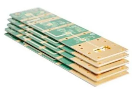
ตัวอย่างแผง PCB
Five PCB examples, with the materials, stack-ups and fabrication decisions behind them.
Special processes follow the application
For communications and RF equipment, a design may need a hybrid stack-up, controlled impedance and back drilling. A power electronics board may instead call for heavier copper, a metal base or embedded copper. A flexible circuit for imaging or a sensor assembly may use a stiffener or shielding film only where the mechanical design calls for it.
The examples cover boards for communications, servers, automotive electronics, industrial control, imaging and medical electronics. These applications help frame the engineering questions. For example, a server board may need a low-loss laminate and a carefully defined via structure, while an industrial connector can depend on how rigid and flexible layers are joined.
Five board examples and the decisions behind them
77 GHz radar PCB
The 18-layer sample combines TSM-DS3, FR28 prepreg and S1000-2M. Its blind and buried vias, ENIG finish and five back-drill groups make the drill plan as important as the laminate selection. Each drill group needs a defined layer target.
เรียนรู้เพิ่มเติมLow-loss material and blind viasHigh-speed server PCB
This 18-layer MEGTRON 8 board is 3.1 mm thick, with a 0.15 mm minimum hole and full-board hard gold. The combination of blind vias, board thickness and finish needs to be confirmed as one fabrication scope.
เรียนรู้เพิ่มเติม4R + 4F + 4R stack-upRigid-flex PCB for an industrial connector
The 12-layer sample combines ITEQ IT-180 and DuPont AP9141R and has a finished thickness of 1.6 mm. The stack-up identifies how the four flexible layers run between the rigid sections, so the transition can be reviewed before lamination.
เรียนรู้เพิ่มเติมRT5880 and laser profilingMillimeter-wave antenna PCB
The eight-layer sample uses Rogers RT5880, a 3 µm soft-gold finish and laser profiling. The drawing needs to carry both the finish requirement and the agreed outline, alongside the material and layer construction.
เรียนรู้เพิ่มเติมHybrid board with an embedded copper section5G base-station power amplifier PCB
This four-layer design combines RO4350B and FR-4 with blind vias, a stepped cavity and a partially embedded copper block. The drawing needs to locate the cavity and copper block relative to the surrounding layers and drilled features.
เรียนรู้เพิ่มเติม