


Industrial Support · Engineering
PCB Impedance Engineering and Stack-Up Review
Use signal and reference layers, material thickness and trace geometry to evaluate target impedance and verification methods.
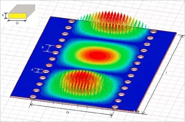
Provide the conditions behind each target
Specify single-ended or differential requirements, tolerances, reference layers, line geometry and materials. Note which design dimensions are allowed to change during review.
Trace a substitution to the affected lines
When laminate or dielectric thickness changes, identify the affected layers and revisit trace width or spacing. Agree on measurement and reporting before releasing the revision.
- Targets and tolerances
- Stack-up and dielectric
- Trace geometry
- Verification method
Inputs and outputs
| Inputs | Outputs |
|---|---|
| Stack-up | Engineering review of the construction |
| Target impedance and tolerance | Proposed geometry |
| Trace geometry and reference plane | Confirmation questions |
| Material properties | Agreed test method and coupons |
Impedance tolerance by board type
Typical applications
High-speed digital boards
RF designs
Mixed-signal products
Impedance Engineering FAQs
Can you calculate geometry for me?
Engineering can propose geometry for review during the project.
Will you change my trace widths?
Only with your approval.