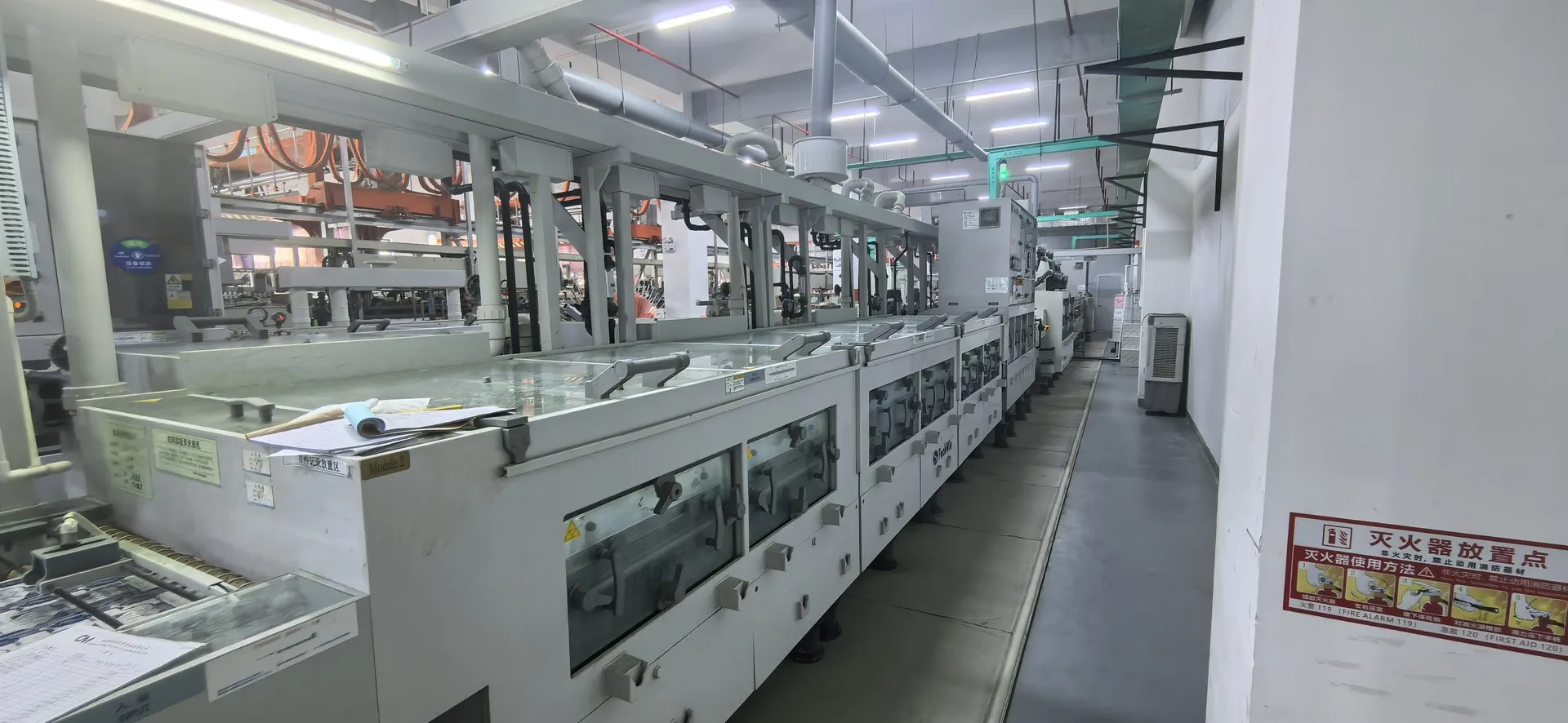

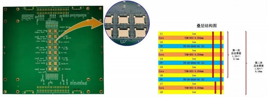
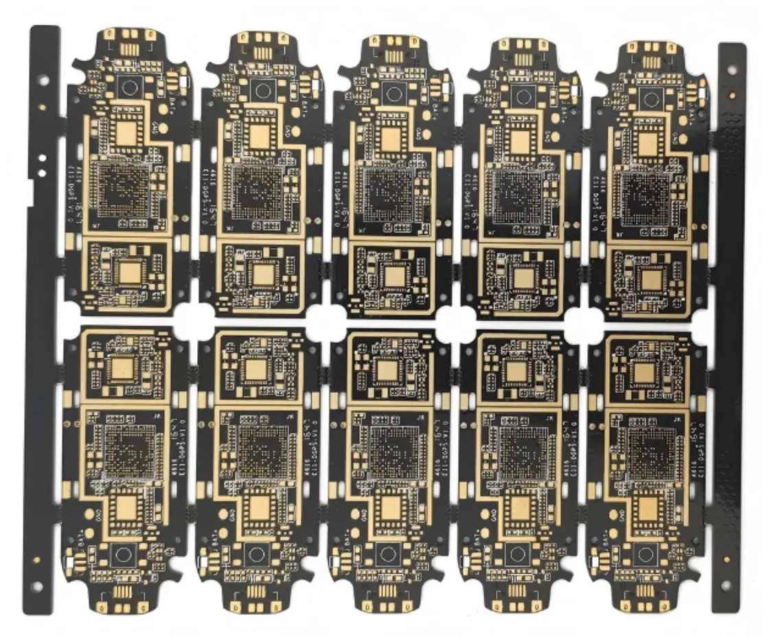
77 GHz radar high-frequency board
- Layers
- 18
- Materials
- TSM-DS3 + FR28 prepreg + S1000-2M, hybrid lamination
- Finish
- Immersion gold (ENIG)
- Special process
- Blind and buried vias, controlled impedance and 5 back-drill groups
Use operating frequency, loss targets and RF layer location to compare laminate, copper and hybrid stack-up options.
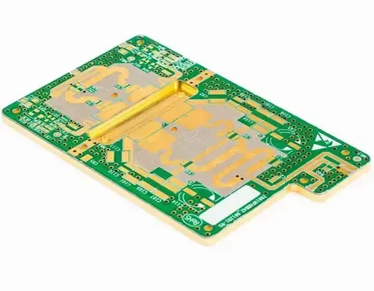
Specify the dielectric properties and frequency you need, plus any copper, thickness or impedance report requirements. Show which layers use RF laminate and which use FR-4.
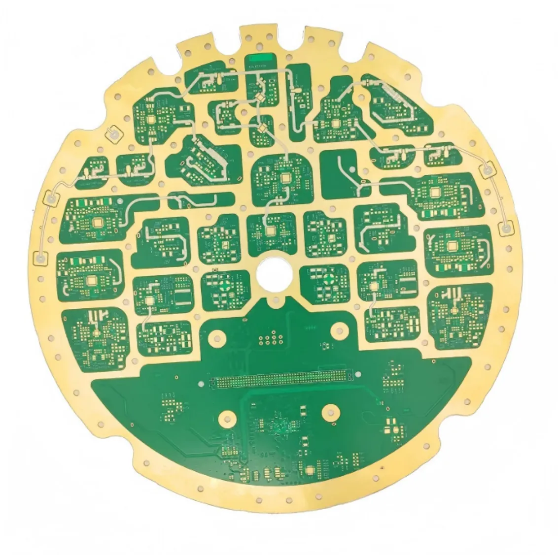
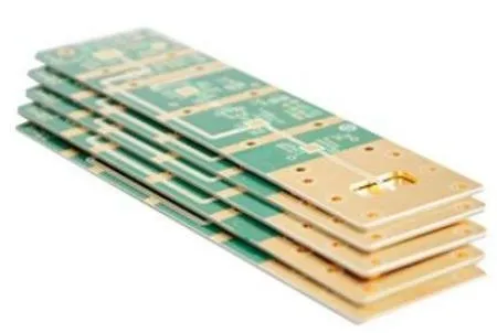
An eight-layer millimeter-wave antenna sample uses Rogers RT5880 and laser profiling. A 5G amplifier sample combines RO4350B and FR-4 with a step cavity and local embedded copper.
| Parameter | Prototype | Mass production |
|---|---|---|
| Material system | PTFE + ceramic, PTFE + glass fiber + ceramic, PTFE + glass fiber | PTFE + ceramic, PTFE + glass fiber + ceramic, PTFE + glass fiber |
| Layer count (max) | 24L | 20L |
| Panel size (max) | 850 × 700 mm | 720 × 650 mm |
| Profile tolerance | ±0.05 mm | ±0.10 mm |
| Slot tolerance | Normal slot ±0.08 mm, short slot ±0.10 mm | Normal slot ±0.10 mm, short slot ±0.13 mm |
| Layer registration | 2 mil | 3 mil |
| Hybrid lamination | PTFE + hydrocarbon ceramic + FR-4 | PTFE + hydrocarbon ceramic + FR-4 |
| Min hole size | 0.075 mm | 0.10 mm |
| Min hole-wall spacing | 0.20 mm | 0.25 mm |
| Hole diameter tolerance | ±0.05 mm | ±0.075 mm |
| Max aspect ratio | 16:1 | 12:1 |
| Hole copper uniformity | COV ≤ 5% | COV ≤ 7% |
| Resin-filled via aspect ratio | 12:1 | 12:1 |
| Resin-filled via type | Through holes, blind and buried vias | Through holes, blind and buried vias |
| Trace width tolerance | ±0.6 mil | ±1 mil |
| Impedance tolerance | ±5% | ±8% |
| Warpage | 0.50% | 0.75% |
| Special processes | POFV (VIPPO), hybrid and local hybrid lamination, long/short, stepped and segmented gold fingers, stepped slots, back drilling, sidewall metallization, N+N, double-sided press-fit mechanical blind vias, local thick copper, high-temperature lamination, copper/silver paste via filling, skip vias, HDI | POFV (VIPPO), hybrid and local hybrid lamination, long/short, stepped and segmented gold fingers, stepped slots, back drilling, sidewall metallization, N+N, double-sided press-fit mechanical blind vias, local thick copper, high-temperature lamination, copper/silver paste via filling, skip vias, HDI |
| Material brands | Shengyi, ITEQ, TUC, Panasonic (M4/M6/M7/M8), Rogers, Taconic, Wangling, 睿龙, 国能 | Shengyi, ITEQ, TUC, Panasonic (M4/M6/M7/M8), Rogers, Taconic, Wangling, 睿龙, 国能 |
Prototype and mass-production values are listed separately and are not interchangeable. Every value is confirmed against your files, the selected material and the assigned facility during engineering review.
Compare stack-up, hole geometry and inspection requirements with your design.
Start with the details you have — engineering will request anything else needed for the review.
Gerber files, BOMs and drawings are handled privately and shared within your project.
It depends on frequency, loss budget, thermal needs and cost. Share your targets and we will review suitable options.
Hybrid stack-ups are reviewed per project for compatibility and processing.