

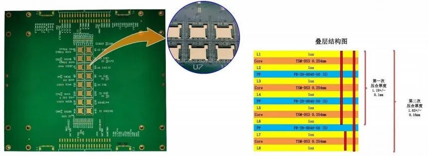
77 GHz radar high-frequency board
- Layers
- 18
- Materials
- TSM-DS3 + FR28 prepreg + S1000-2M, hybrid lamination
- Finish
- Immersion gold (ENIG)
- Special process
- Blind and buried vias, controlled impedance and 5 back-drill groups
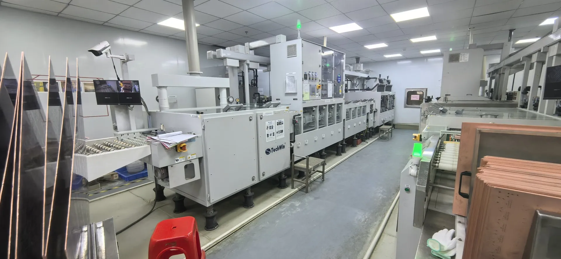
Plan BGA escape routing with each via's layer span, diameter, pad and fill requirements. Check the lamination sequence as part of the stack-up.
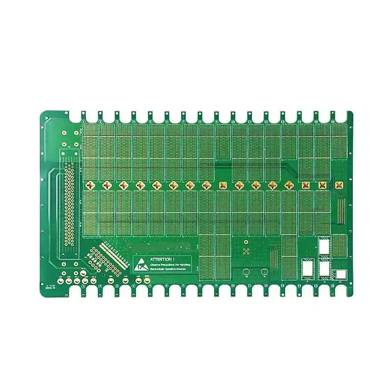
Separate stacked, staggered and via-in-pad structures. Provide a drill map by layer span and specify any fill, cap and planarity requirements at component pads.
The published rigid PCB minimum blind via diameter is 0.05 mm for prototypes and 0.075 mm for production. Published minimum trace and space are 2.5 mil each for prototypes and 3 mil each for production. Confirm the combination against the actual stack-up.
| Parameter | Prototype | Mass production |
|---|---|---|
| Rigid — HDI level | 9th order | 5th order |
| Rigid — Min trace / space | 2.5 / 2.5 mil | 3 / 3 mil |
| Rigid — Min blind via diameter | 0.05 mm | 0.075 mm |
| Rigid — Min through-hole diameter | 0.075 mm | 0.10 mm |
| Rigid — Layer registration accuracy | 0.8 mil | 1 mil |
| Rigid — Max aspect ratio | 35:1 | 30:1 |
| Rigid — Impedance control tolerance | ±5% | ±7% |
| FPC — HDI capability | 4-layer any-layer interconnect | 6-layer any-layer interconnect |
| FPC — Min BGA pitch | 150 µm | 100 µm |
| FPC — Min blind via diameter | 0.05 mm | 0.05 mm |
Prototype and mass-production values are listed separately and are not interchangeable. Every value is confirmed against your files, the selected material and the assigned facility during engineering review.
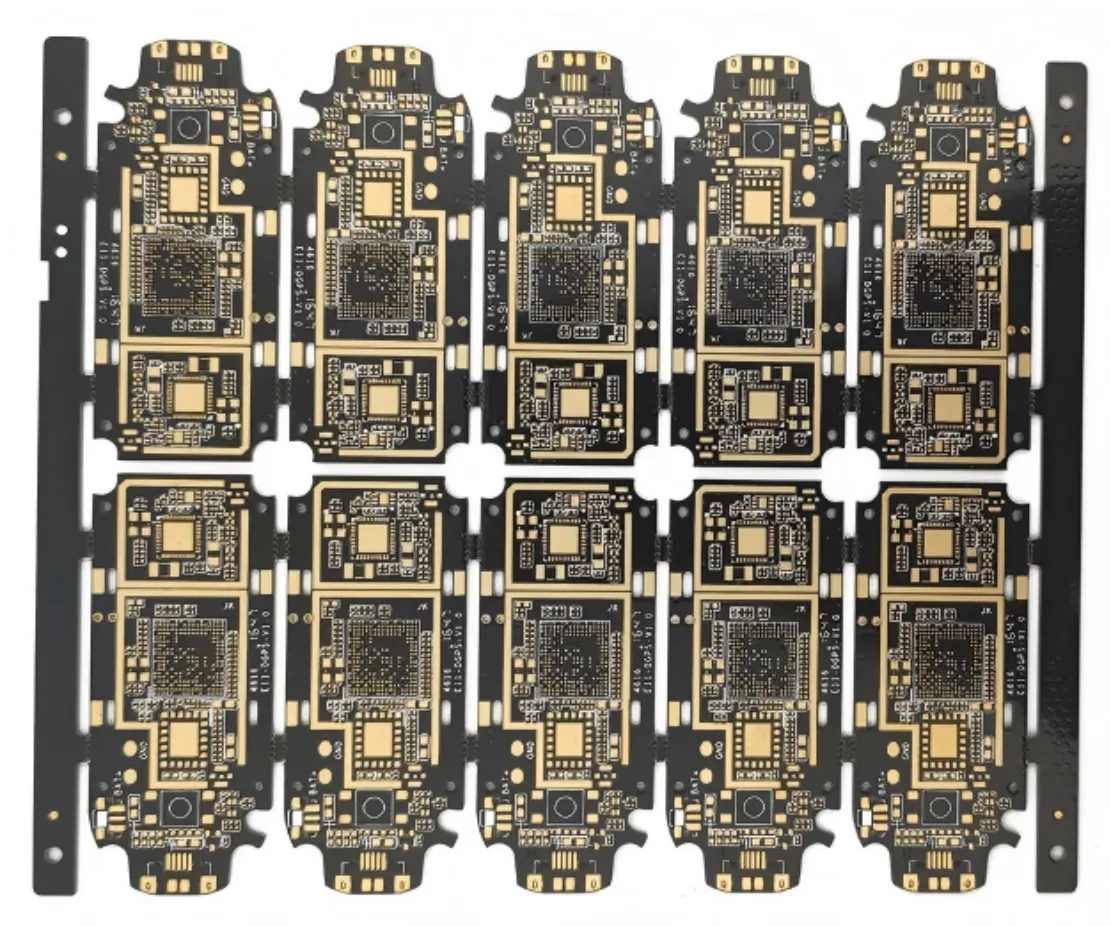
Start with the details you have — engineering will request anything else needed for the review.
Gerber files, BOMs and drawings are handled privately and shared within your project.
Via structures are reviewed per design. Engineering confirms the feasible structure before quotation.
HDI adds process steps, but it can reduce layer count or board size. We explain the trade-offs during review.