
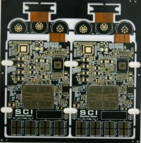
12-layer rigid-flex board
- Structure
- 12 layers, 4R + 4F + 4R
- Materials
- ITEQ IT-180 + DuPont AP9141R
- Thickness / min hole
- 1.6 mm / 0.2 mm
- Finish
- Immersion gold (ENIG)
- Application
- High-end industrial connector
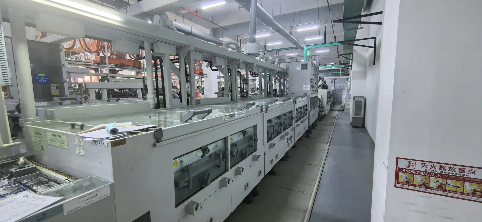
Define the rigid sections, flex zones and transitions in the installed position. Specify coverlay, stiffeners and any assembly support.
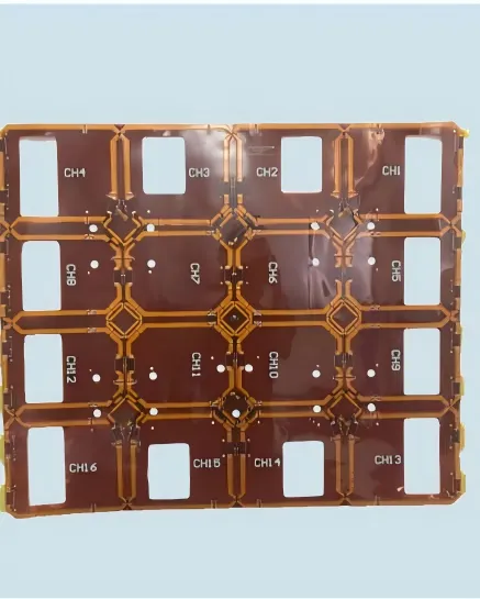
Mark bend direction, radius and connector position. Identify coverlay openings and stiffener boundaries where soldering or support is needed.
A 12-layer industrial connector sample uses a 4R + 4F + 4R stack with ITEQ IT-180 and DuPont AP9141R. It has a 1.6 mm thickness and 0.2 mm minimum hole. Use your installed geometry to review the applicable stack.
| Parameter | Prototype | Mass production |
|---|---|---|
| Layer count (max) | 20L | 18L |
| Panel size | 400 × 540 mm | 400 × 540 mm |
| Finished board thickness | 0.25–5.0 mm | 0.25–3.2 mm |
| Min trace / space | 1.5 / 1.5 mil | 2 / 2 mil |
| Min hole-to-trace clearance | 4 mil | 5 mil |
| Copper weight | 1/3–3 oz | 1/3–2 oz |
| Layer registration accuracy | 0.8 mil | 1 mil |
| Min through-hole diameter | 0.075 mm | 0.10 mm |
| Min blind via diameter | 0.05 mm | 0.05 mm |
| Max aspect ratio | 16:1 | 12:1 |
| Etching tolerance | ±10% / ±0.8 mil | ±10% / ±1 mil |
| Min solder mask bridge | 2 mil | 3 mil |
| Impedance control tolerance | ±5% | ±7% |
| Surface finish | ENIG, electrolytic gold, HASL, Ni/Pd/Au, thick electrolytic gold, immersion tin, immersion silver, OSP, carbon | ENIG, electrolytic gold, HASL, Ni/Pd/Au, thick electrolytic gold, immersion tin, immersion silver, OSP |
| Supported structures | Symmetrical single-sided flex, multilayer flex, flex gold fingers, air gap, asymmetrical stack-up, HDI, outer-layer flex with press-fit, bookbinder, high-frequency and high-speed | Symmetrical single-sided flex, multilayer flex, flex gold fingers, air gap, asymmetrical stack-up, HDI, outer-layer flex with press-fit, bookbinder, high-frequency and high-speed |
| Material types | Shengyi, 宏仁, 台虹, DuPont, Panasonic, Rogers, ITEQ | Shengyi, 宏仁, 台虹, DuPont, Panasonic, Rogers, ITEQ |
Prototype and mass-production values are listed separately and are not interchangeable. Every value is confirmed against your files, the selected material and the assigned facility during engineering review.
| Parameter | Prototype | Mass production |
|---|---|---|
| Layer count (max) | 12 | 16 |
| Min dielectric thickness | 12.5 µm | 12.5 µm |
| Min BGA pitch | 150 µm | 100 µm |
| Min board thickness | 50 µm | 50 µm |
| Max panel size | 610 × 1200 mm | 610 × 1200 mm |
| Base copper thickness | 9–35 µm | 6–35 µm |
| Min trace / space | 40 / 40 µm | 35 / 35 µm |
| Pattern registration tolerance | ±50 µm | ±20 µm |
| Min pattern-to-edge clearance | 0.10 mm | 0.07 mm |
| Etching tolerance | ±20 µm | ±15 µm |
| Min through-hole diameter | 0.10 mm | 0.075 mm |
| Min blind via diameter | 0.05 mm | 0.05 mm |
| Hole position tolerance | ±0.05 mm | ±0.05 mm |
| Impedance control tolerance | ±10% | ±5% |
| Outline tolerance | ±0.10 mm | ±0.05 mm |
| Surface finish | HASL, ENIG, immersion silver, OSP, Ni/Pd/Au, electrolytic gold | HASL, ENIG, immersion silver, OSP, Ni/Pd/Au, electrolytic gold |
| Stiffener type | FR-4, PI, stainless steel | FR-4, PI, stainless steel |
| Stiffener registration tolerance | ±0.20 mm | ±0.10 mm |
| HDI capability | 4-layer any-layer interconnect | 6-layer any-layer interconnect |
| LCP material | Supported | Supported |
Prototype and mass-production values are listed separately and are not interchangeable. Every value is confirmed against your files, the selected material and the assigned facility during engineering review.
Start with the details you have — engineering will request anything else needed for the review.
Gerber files, BOMs and drawings are handled privately and shared within your project.
Mark the rigid and flexible areas, bend locations and any stiffeners, together with the layer construction.
Yes. Assembly needs are reviewed with the construction so the board can be supported during assembly.