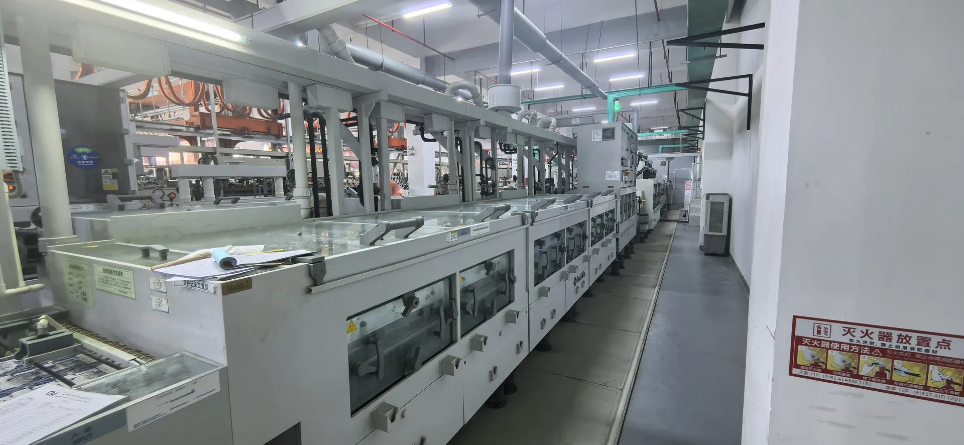

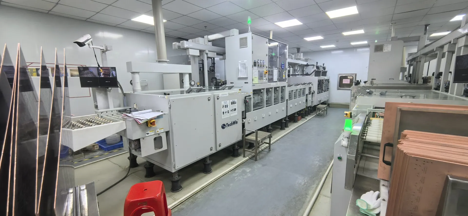
Multilayer PCB Stack-Up and Fabrication
Define the power, signal and reference layers together with drilling and copper distribution. Confirm the stack before releasing the fabrication data.
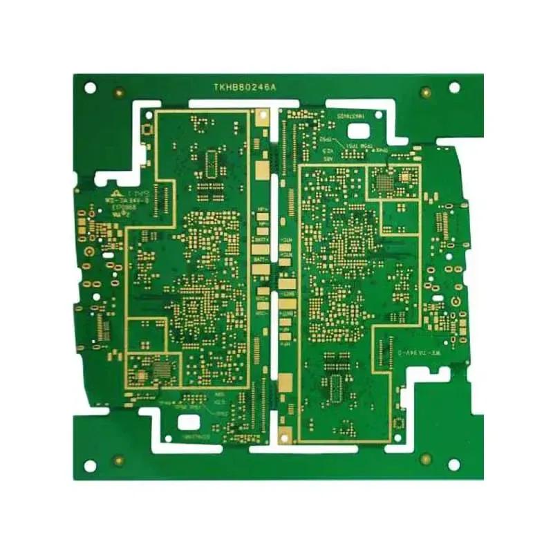
Map impedance lines to their references
List targets, signal layers and reference planes. If the layer order or laminate changes, recheck dielectric thickness, trace geometry and the affected requirements.
Reconcile each drill span with the stack
Provide separate start and stop layers for blind and buried groups, plus finished hole dimensions and tolerances. Use the same revision for the layer schedule and drill files.
- Layer structure and stack-up against your targets
- Material and thickness for the application
- Drill and via strategy
- Copper balance and registration considerations
Multilayer capability
| Parameter | Prototype | Mass production |
|---|---|---|
| Layer count (max) | 50L | 36L |
| Finished board thickness | 0.2–15.0 mm | 0.3–7.0 mm |
| Thickness tolerance | ±8% | ±8% |
| Min trace / space | 2.5 / 2.5 mil | 3 / 3 mil |
| Min hole-to-trace clearance | 5 mil | 5 mil |
| Copper weight | 1/3–12 oz | 1/3–8 oz |
| Layer registration accuracy | 0.8 mil | 1 mil |
| Min through-hole diameter | 0.075 mm | 0.10 mm |
| Max aspect ratio | 35:1 | 30:1 |
| Impedance control tolerance | ±5% | ±7% |
| Surface finish | ENIG, electrolytic gold, HASL, Ni/Pd/Au, thick electrolytic gold, immersion tin, immersion silver, OSP, carbon | ENIG, electrolytic gold, HASL, Ni/Pd/Au, thick electrolytic gold, immersion tin, immersion silver, OSP, carbon |
| Material types | Shengyi, TUC, 建涛, Nan Ya, ITEQ, Rogers, 华正, Elite Material (EMC), Isola (Tg135 / Tg150 / Tg170, CAF resistance, CTI > 600, halogenated and halogen-free) | Shengyi, TUC, 建涛, Nan Ya, ITEQ, Rogers, 华正, Elite Material (EMC), Isola (Tg135 / Tg150 / Tg170, CAF resistance, CTI > 600, halogenated and halogen-free) |
Prototype and mass-production values are listed separately and are not interchangeable. Every value is confirmed against your files, the selected material and the assigned facility during engineering review.
Typical applications
Industrial controllers and instruments
Communication and networking hardware
Automotive and power electronics modules
What to send for a PCB review
Start with the details you have — engineering will request anything else needed for the review.
Files and details for a PCB review
- Gerber (RS-274X) or ODB++ data with drill files
- Fabrication drawing with material, thickness and finish
- Stack-up and impedance targets, if any
- Quantity for prototype and for production
- Special requirements such as IPC class, testing or packaging
Technical files stay private
Gerber files, BOMs and drawings are handled privately and shared within your project.
Multilayer PCB FAQs
Can you propose a stack-up for my design?
Yes. Share your layer count, thickness and impedance targets, and engineering will propose or check a stack-up during review.
Are prototype and production builds reviewed the same way?
Both are reviewed, but prototype and production requirements are kept separate so the production build is confirmed on its own terms.