


PCB Controlled Impedance and Verification
Pair each impedance target with a signal layer, reference plane and tolerance. Recheck trace geometry when the material or thickness changes.
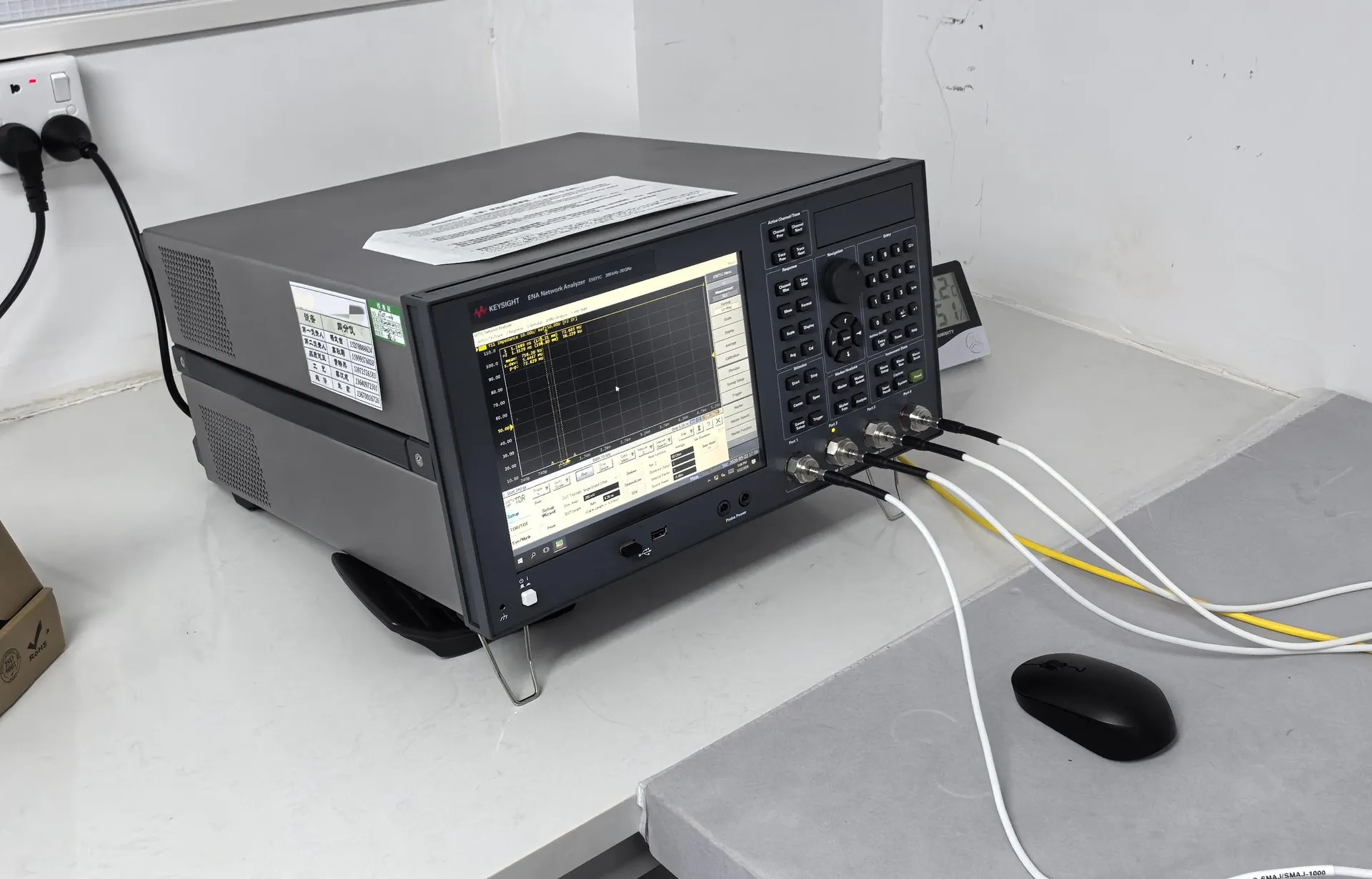
Give the impedance schedule layer context
Identify single-ended and differential targets, trace widths, spacing and reference layers. An archived project provides the impedance schedule and stack together so each requirement can be checked against its actual layer.
Specify how the board will be accepted
Indicate the line groups, test structure and records required. When a laminate or copper thickness changes, recheck the affected groups before release.
- Impedance targets and tolerances
- Trace width and spacing
- Dielectric thickness and material
- Test coupons and method
Engineering tools
Impedance tolerance by board type
| Parameter | Prototype | Mass production |
|---|---|---|
| Rigid — Impedance control tolerance | ±5% | ±7% |
| Rigid-flex — Impedance control tolerance | ±5% | ±7% |
| FPC — Impedance control tolerance | ±10% | ±5% |
| High-frequency / high-speed — Impedance tolerance | ±5% | ±8% |
| High-frequency / high-speed — Trace width tolerance | ±0.6 mil | ±1 mil |
| Factory general — impedance tolerance | ±10% | ±10% |
Prototype and mass-production values are listed separately and are not interchangeable. Every value is confirmed against your files, the selected material and the assigned facility during engineering review.
Typical applications
High-speed digital interfaces
RF transmission lines
USB
Ethernet and memory buses
What to send
Helpful details for advanced designs
- Target frequency, data rate and loss budget
- Impedance targets and tolerances
- Preferred or approved materials
- Via structure and back drilling layers
- Test and inspection requirements
Start a project
Send your files and planned quantities. We will confirm the open engineering points before quoting.
Controlled Impedance FAQs
Can you adjust trace widths?
Engineering may propose geometry adjustments to meet your targets, and changes are confirmed with you before production.
Do you guarantee impedance?
Targets and the test method are agreed in the quotation. No performance value is assumed without project review.