
High-Speed PCBs with Low-Loss Stack-Ups and Back Drilling
Start with data rate, loss budget and impedance. Confirm reference planes, geometry and acceptable via stubs against that budget.
Select materials against the link requirement
Compare laminate data under its specified test conditions. Copper, trace geometry and dielectric thickness also affect the finished transmission line.
Locate each back-drilled group
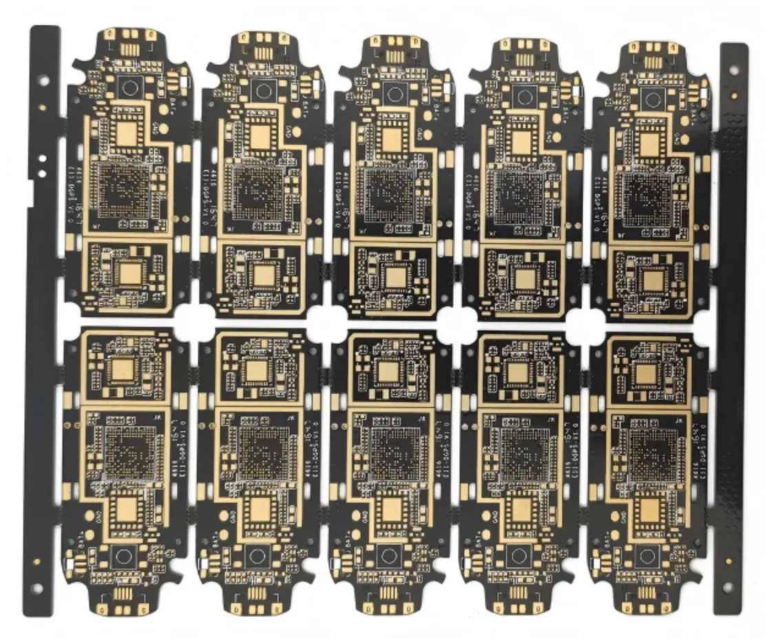
Specify entry side, target layer, allowed stub and connections to protect. A company sample uses an 18-layer MEGTRON 8 stack, illustrating how hole size, thickness and material can constrain the same build.
- Low-loss material options
- Impedance targets and trace geometry
- Via stubs and back drilling
- Stack-up symmetry and reference planes
Engineering tools
High-speed capability
| Parameter | Prototype | Mass production |
|---|---|---|
| High-frequency / high-speed — Layer count (max) | 24L | 20L |
| High-frequency / high-speed — Impedance tolerance | ±5% | ±8% |
| Trace width tolerance | ±0.6 mil | ±1 mil |
| Layer registration | 2 mil | 3 mil |
| Max aspect ratio | 16:1 | 12:1 |
| Hole copper uniformity | COV ≤ 5% | COV ≤ 7% |
| Warpage | 0.50% | 0.75% |
| Special processes | POFV (VIPPO), hybrid and local hybrid lamination, long/short, stepped and segmented gold fingers, stepped slots, back drilling, sidewall metallization, N+N, double-sided press-fit mechanical blind vias, local thick copper, high-temperature lamination, copper/silver paste via filling, skip vias, HDI | POFV (VIPPO), hybrid and local hybrid lamination, long/short, stepped and segmented gold fingers, stepped slots, back drilling, sidewall metallization, N+N, double-sided press-fit mechanical blind vias, local thick copper, high-temperature lamination, copper/silver paste via filling, skip vias, HDI |
| Rigid — Layer count (max) | 50L | 36L |
| Rigid — Impedance control tolerance | ±5% | ±7% |
Prototype and mass-production values are listed separately and are not interchangeable. Every value is confirmed against your files, the selected material and the assigned facility during engineering review.
Typical applications
Servers
storage and accelerators
Networking and switching equipment
Test and measurement hardware
What to send for a PCB review
Start with the details you have — engineering will request anything else needed for the review.
Files and details for a PCB review
- Gerber (RS-274X) or ODB++ data with drill files
- Fabrication drawing with material, thickness and finish
- Stack-up and impedance targets, if any
- Quantity for prototype and for production
- Special requirements such as IPC class, testing or packaging
Technical files stay private
Gerber files, BOMs and drawings are handled privately and shared within your project.
High-Speed PCB FAQs
Do you test impedance?
The impedance test method is agreed with the order during review.
Can you help reduce loss?
Engineering can review material and geometry options against your loss budget. No performance value is assumed without project review.