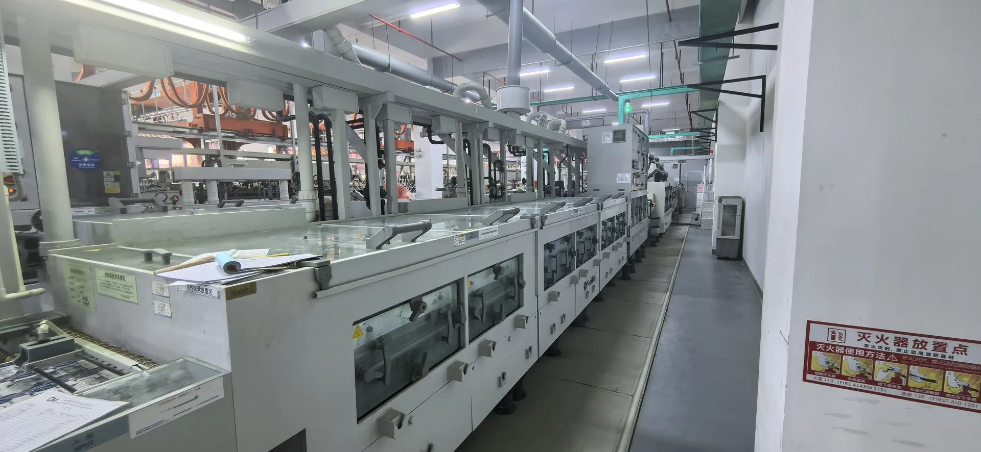

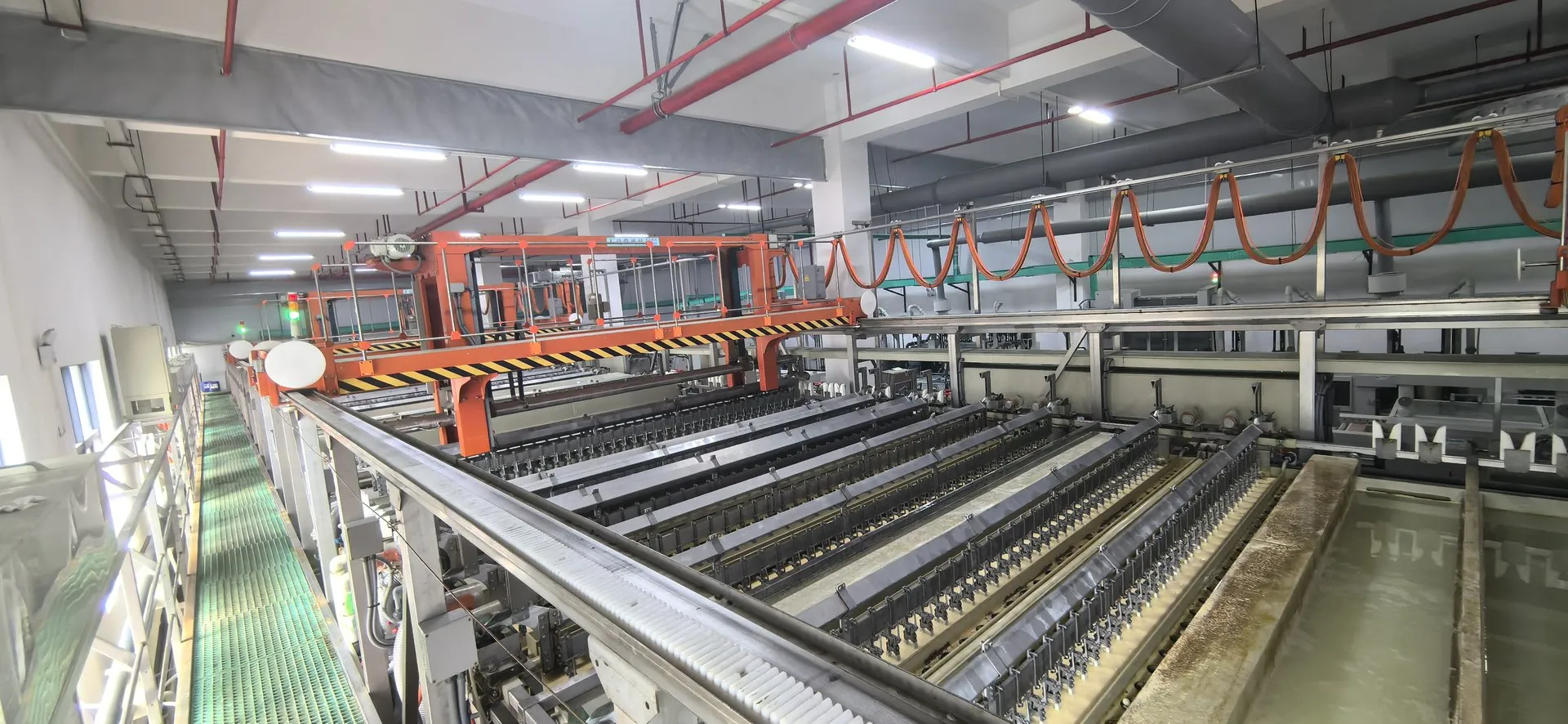
PCB Processes and Capability by Production Stage
Compare rigid, rigid-flex, FPC and high-frequency or high-speed capabilities against your own stack-up and drill requirements.
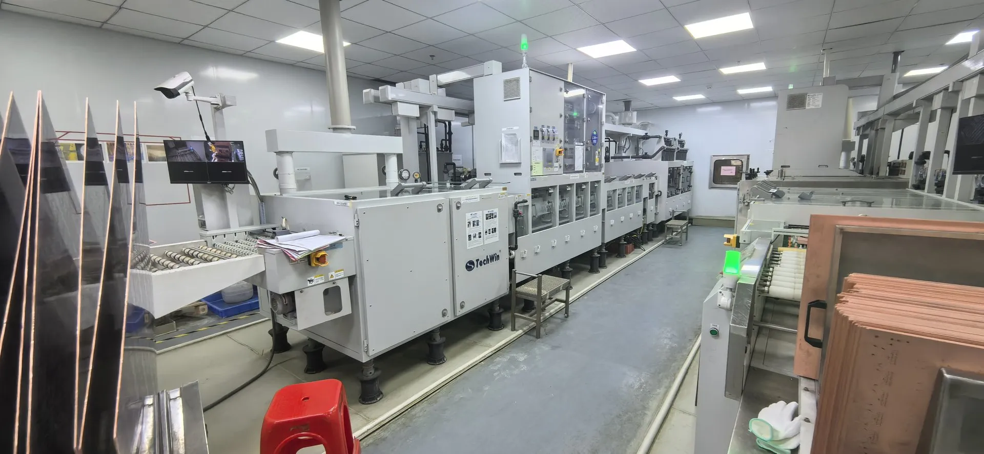
Read the right column for your build
Published rigid PCB limits are 50 layers for prototypes and 36 for production. Minimum trace and space are 2.5 mil each for prototypes and 3 mil each for production. Use the table for your board type and review the material and hole combination.
Carry acceptance from the drawing into the order
Specify lamination, drilling and surface treatment on the approved revision. If you need continuity testing, impedance records or cross sections, identify the targets and records.
Rigid PCB manufacturing flow
The process runs from laminate preparation through electrical test and final inspection.
Cutting
Laminate panels cut to working size.
Inner-layer imaging
Inner-layer patterns imaged and etched, then checked by AOI.
Lamination
Cores and prepregs pressed into the multilayer stack.
Drilling
Mechanical and laser drilling of holes and vias.
Plating
Hole metallization and copper plating.
Outer-layer imaging
Outer-layer patterns imaged, etched and checked by AOI.
Solder mask & legend
Solder mask and silkscreen applied.
Surface finish
ENIG, hard gold, immersion tin or silver, OSP and others.
Profiling
Routing, V-cut and outline machining.
Electrical test & final inspection
Flying-probe or fixture test, final inspection and packing.
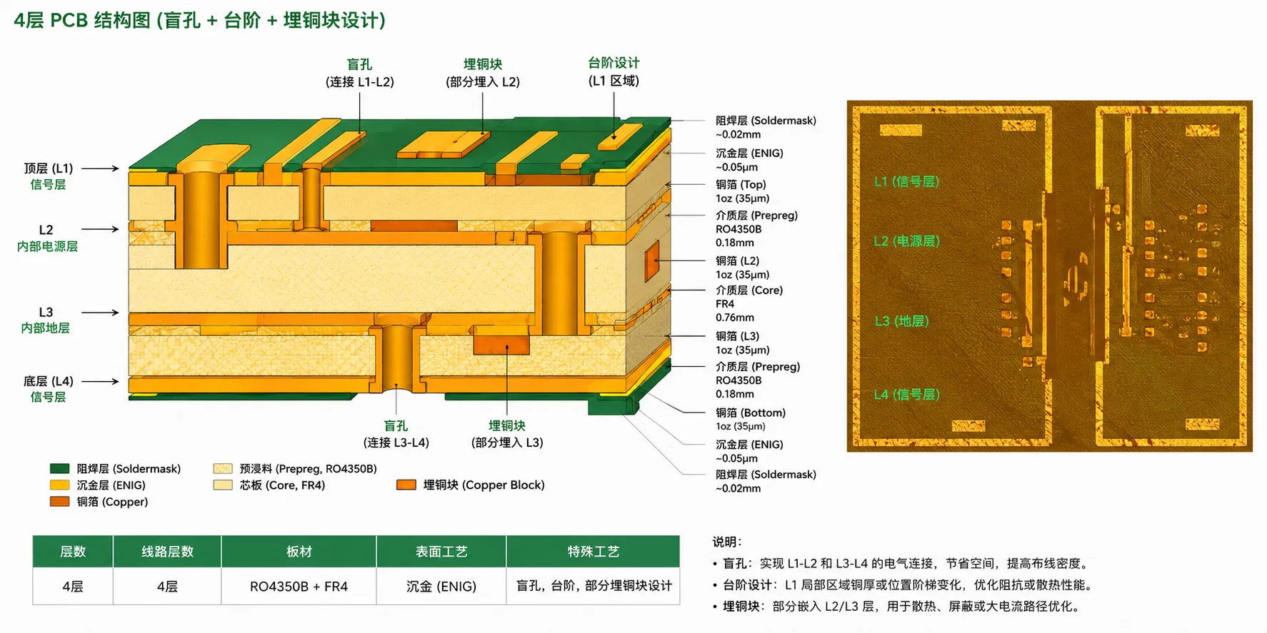
Rigid-flex boards bring two constructions together
The rigid-flex process prepares the FR-4 rigid section, flexible copper-clad laminate, coverlay and other lamination materials along separate paths. The flexible circuit is patterned and inspected before the coverlay is applied. The rigid and flexible sections are then combined in the specified order and laminated.
After lamination, the process uses X-ray for target location before subsequent drilling and profiling. The agreed construction determines where to remove material or control routing depth so the flexible section can be released. The board then goes through electrical test, final quality inspection and packing.
A rigid-flex drawing therefore needs more than an overall outline. It should show which layers continue through the flex region, where the coverlay and stiffeners sit, and the boundaries between rigid and flexible sections. These details affect both the build sequence and the points checked on the finished board.
What to confirm for each board family
Use the board family and production stage to identify what engineering needs to check.
| Board family | Engineering review points |
|---|---|
| Flexible circuits | Confirm the flex material, copper thickness, coverlay and stiffeners. |
| Conventional rigid boards | Check layer count, finished thickness, trace and space, copper weight, hole size and the required impedance tolerance against the intended construction. |
| Rigid-flex boards | Confirm the rigid and flexible layer arrangement and any air-gap, asymmetric or HDI structure. Review alignment, the coverlay and the flex release process together. |
| High-frequency and high-speed boards | Confirm the material system, hybrid lamination, hole geometry and impedance targets. |