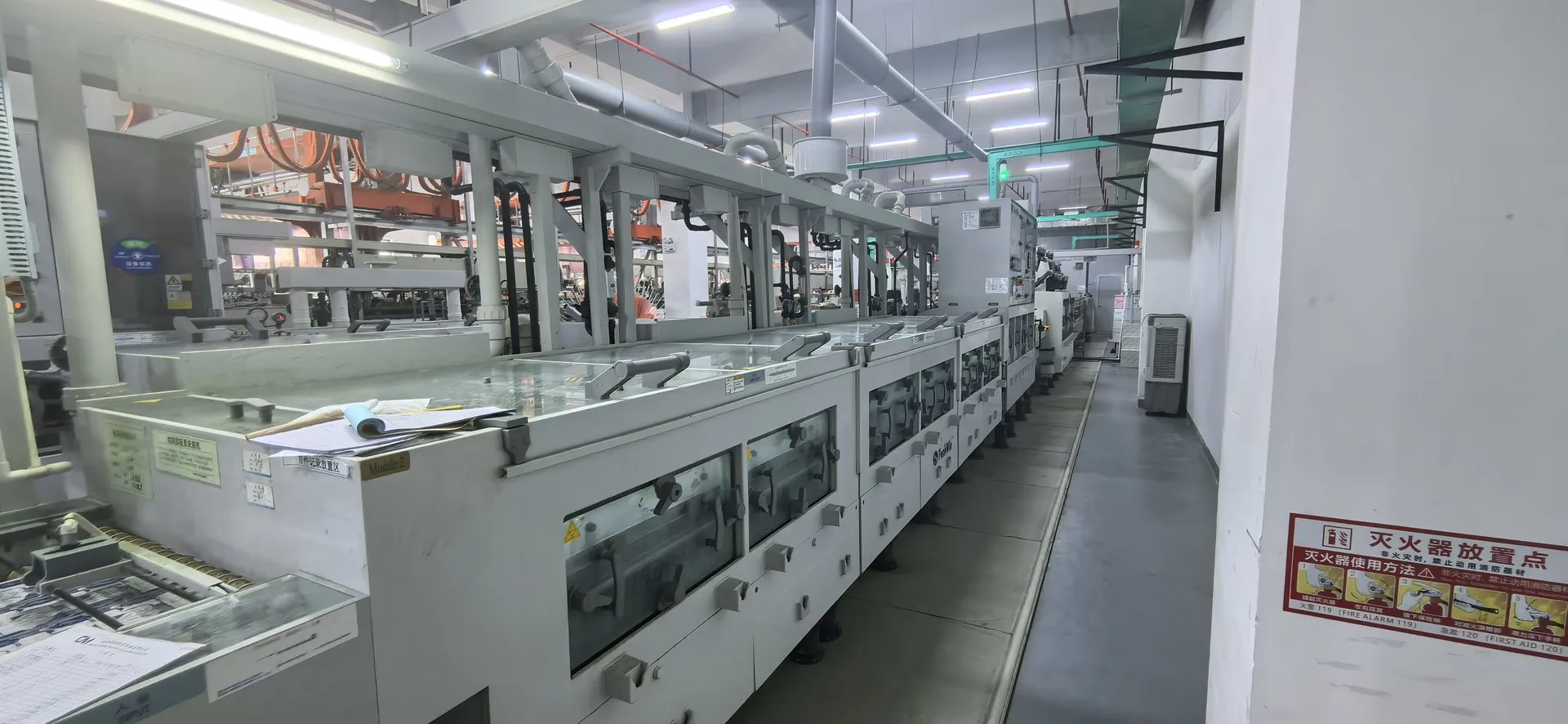

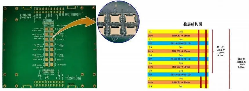
77 GHz radar high-frequency board
- Layers
- 18
- Materials
- TSM-DS3 + FR28 prepreg + S1000-2M, hybrid lamination
- Finish
- Immersion gold (ENIG)
- Special process
- Pure PTFE blind/buried-via impedance board, 5 back-drill groups
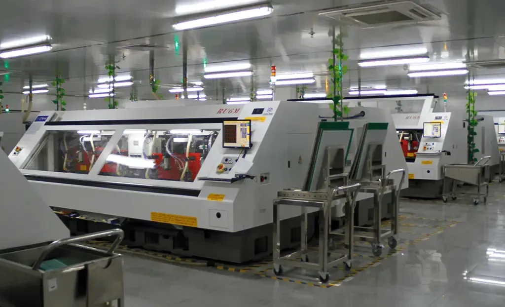
Complex high-layer stack-ups for communication, computing and test equipment.
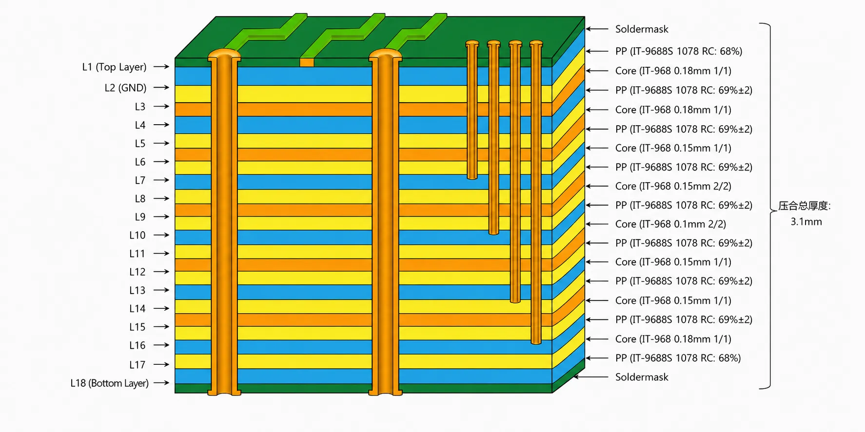
High-layer boards need careful stack-up planning, registration and material selection. We review thickness, layer structure and materials, and confirm the layer count for each project.
| Positioning | Up to 48 Layers | |
|---|---|---|
| Standard / prototype | Advanced / mass production | |
| High Layer Count | Up to 48L | Up to 48L |
Source: ShinePCB capability workbook, navigation overview. Values are confirmed against your files and the assigned facility during engineering review; certificates are available on request.
| Parameter | Prototype | Mass production |
|---|---|---|
| Rigid — Layer count (max) | 48L | 36L |
| Rigid — Finished board thickness | 0.2–15.0 mm | 0.3–7.0 mm |
| Rigid — Layer registration accuracy | 0.8 mil | 1 mil |
| Rigid-flex — Layer count (max) | 20L | 18L |
| FPC — Layer count (max) | 12 | 16 |
| High-frequency / high-speed — Layer count (max) | 24L | 20L |
Source: ShinePCB capability workbook. Prototype and mass-production values are listed separately and are not interchangeable. Every value is confirmed against your files, the selected material and the assigned facility during engineering review. The product line lists multilayer boards from 4 to 48 layers.
Board constructions from the ShinePCB company presentation — not customer references.
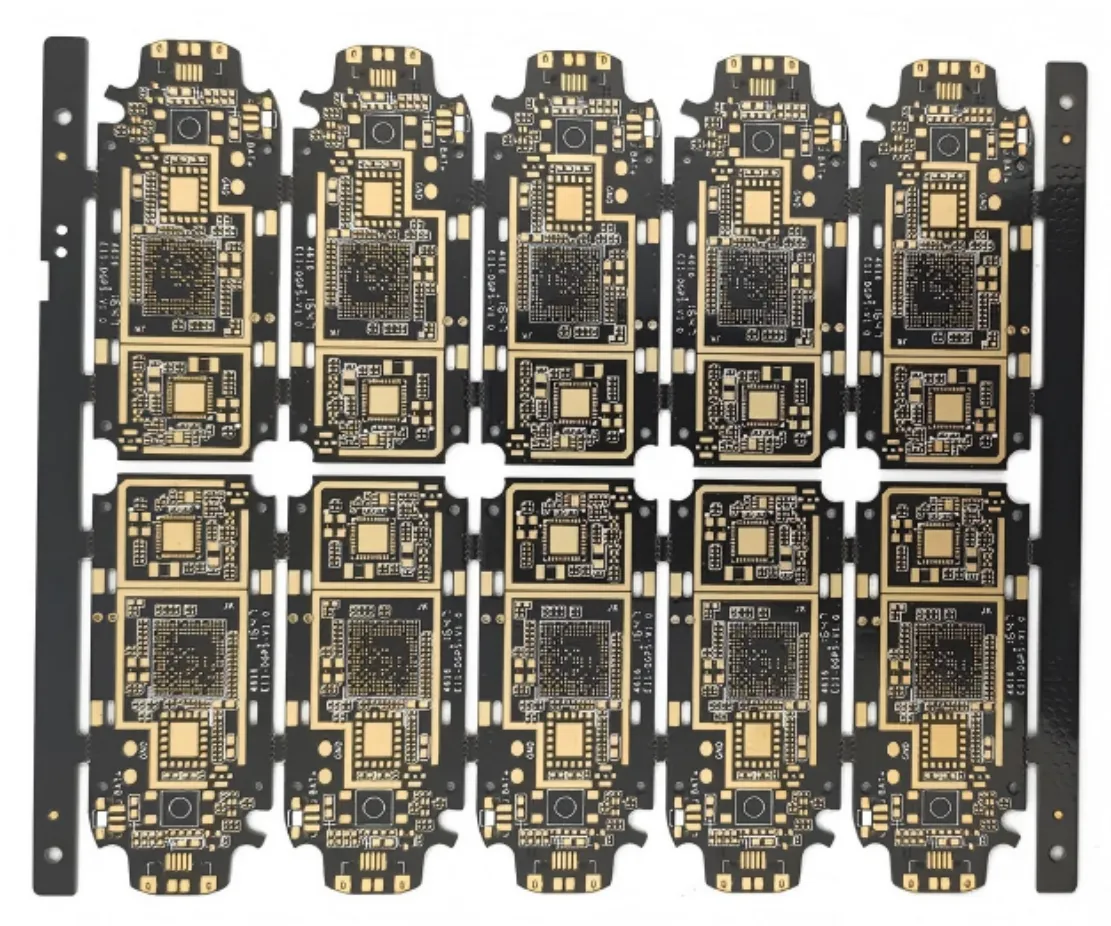
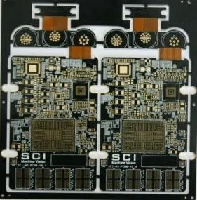
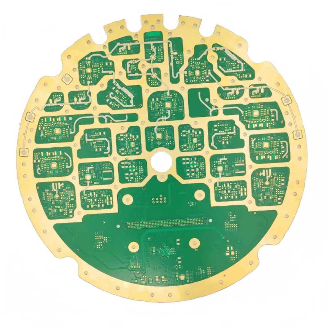
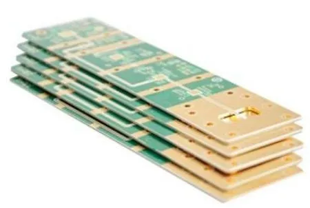
Builds from the ShinePCB company presentation. They illustrate process scope and are not customer references.
Every order follows the same controlled sequence. Prototype and production requirements are reviewed separately.
Gerber or ODB++, drill data, drawing and quantities are checked for completeness.
Open points on manufacturability, materials or special processes are sent before quotation.
Construction, laminate and finish are confirmed with you and written into the order.
The order is released to the facility whose process and qualification fit the requirements.
Inspection and electrical test follow the methods agreed for your order.
Boards are packed and shipped under the confirmed delivery terms.
Start with the details you have — engineering will request anything else needed for the review.
Customer Gerber, BOM and design data are managed under an ISO/IEC 27001 information security system and shared only within your project.
Layer count depends on the complete design and is confirmed in engineering review.
Yes. Send your proposed stack-up and targets for review.