
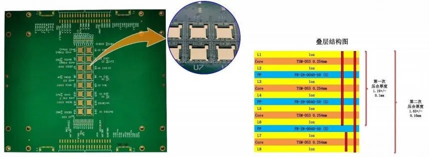
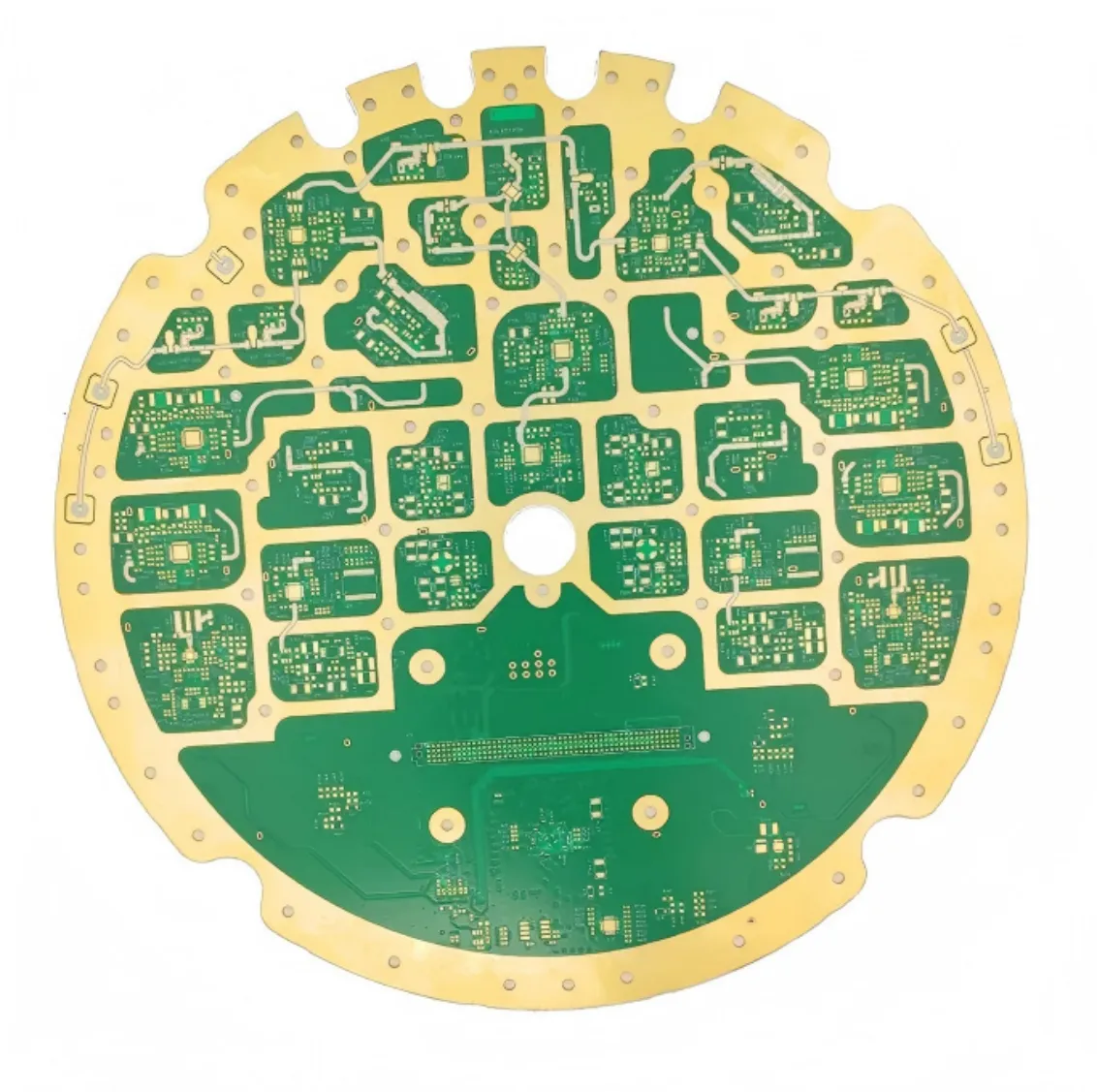
77 GHz radar high-frequency board
- Layers
- 18
- Materials
- TSM-DS3 + FR28 prepreg + S1000-2M, hybrid lamination
- Finish
- Immersion gold (ENIG)
- Special process
- Blind and buried vias, controlled impedance and 5 back-drill groups

Choose microvias, sequential lamination, back drilling or hybrid laminates according to what limits your design.
Dense BGA routing calls for a layer-by-layer via map. A tight stub budget calls for back-drill groups with defined target layers. Hybrid RF and digital sections need their own material and reference-layer requirements.
An 18-layer 77 GHz company sample combines TSM-DS3, FR28 prepreg and S1000-2M with blind and buried vias and five back-drill groups. Submit the stack-up and drill charts together to review the combination.
Advanced structures depend on the full design: stack-up, materials, via strategy and test method. We review these together and confirm feasibility before quotation.
Microvia and fine-line structures for dense BGA breakout and compact products.
Vias that connect only the layers that need them, freeing routing space in multilayer boards.
Removal of unused via stubs to reduce reflections on fast signals.
Trace geometry and dielectric choices matched to your impedance targets.
Multiple lamination cycles for complex via structures and hybrid constructions.
Complex stack-ups for communication, computing and test equipment.
Compare the constructions and inspection requirements with your design.
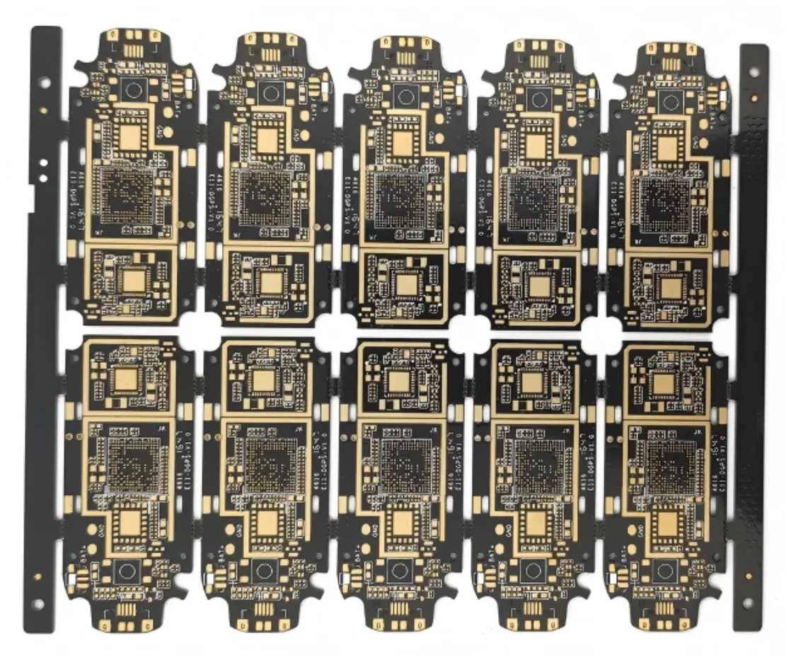
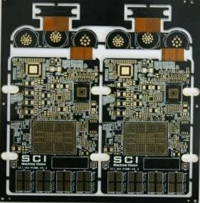
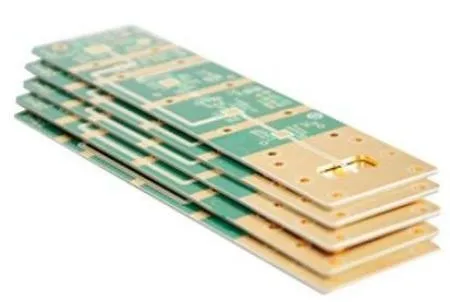
Material choice affects loss, stability, thermal performance and cost. Supplier datasheet values are material data, not fabrication guarantees; we confirm options and availability for each project.
Rogers laminates for RF and microwave circuits.
Isola laminates for high-speed digital and low-loss designs.
PTFE-based materials for demanding RF applications.
FR-4 with a higher glass-transition temperature for designs exposed to heat.
Send your files and planned quantities. We will confirm the open engineering points before quoting.
Hybrid stack-ups are reviewed per project. We confirm compatibility and processing before quotation.
Impedance targets are reviewed with your stack-up and geometry, and the test method is agreed in the quotation. We do not assume a performance value without project review.