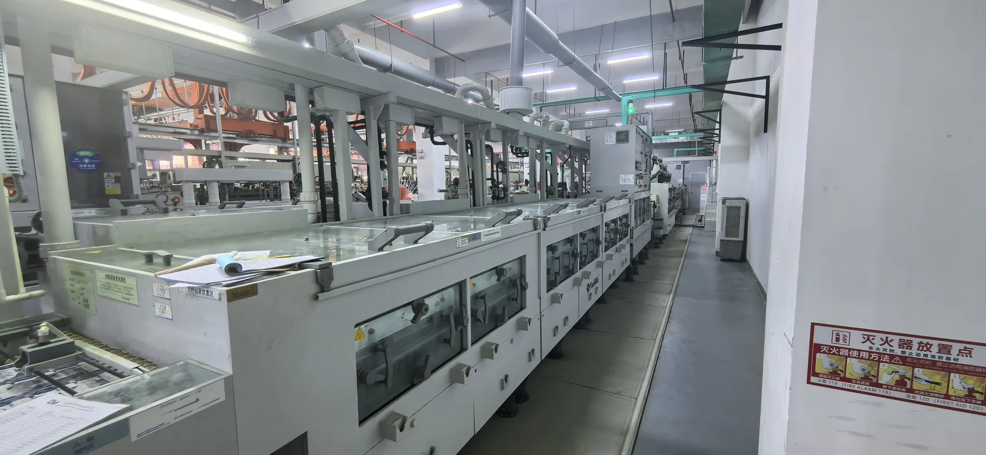

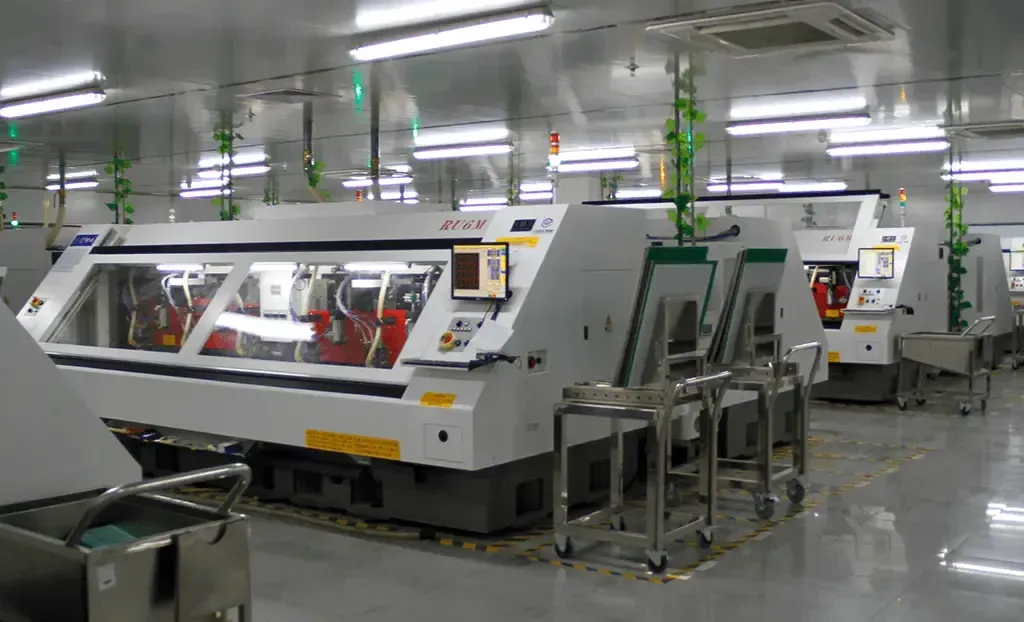
HDI & Microvia
Microvia and fine-line structures for dense BGA breakout and compact products.
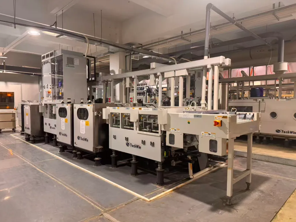
HDI & Microvia with ShinePCB
Microvias connect adjacent layers in a small footprint, enabling fine-pitch components and denser routing. We review via-in-pad, stacked or staggered structures and line widths with your stack-up before quotation.
- Microvia structure and layer pairs
- Via-in-pad and filling
- Fine-line routing
- Lamination sequence
Capability and certificates
| Positioning | Fine Line / High Density | |
|---|---|---|
| Standard / prototype | Advanced / mass production | |
| HDI & Microvia | Trace/Space 1.5/1.5mil; Laser Via 0.05mm | Trace/Space 2/2mil |
Related certificates
- ISO 9001:2015133628
- UL 796E466435
- IECQ QC 080000IECQ-H NQAGB 25.0038
Source: ShinePCB capability workbook, navigation overview. Values are confirmed against your files and the assigned facility during engineering review; certificates are available on request.
HDI and microvia limits
| Parameter | Prototype | Mass production |
|---|---|---|
| Rigid — HDI level | 9th order | 5th order |
| Rigid — Min trace / space | 1.5 / 1.5 mil | 2 / 2 mil |
| Rigid — Min blind / buried via diameter | 0.05 mm | 0.075 mm |
| Rigid — Layer registration accuracy | 0.8 mil | 1 mil |
| Rigid — Etching tolerance | ±10% / ±0.8 mil | ±10% / ±1 mil |
| Rigid-flex — Min laser via diameter | 0.05 mm | 0.05 mm |
| FPC — HDI capability | 4-layer any-layer interconnect | 6-layer any-layer interconnect |
| FPC — Min BGA pitch | 150 µm | 100 µm |
Source: ShinePCB capability workbook. Prototype and mass-production values are listed separately and are not interchangeable. Every value is confirmed against your files, the selected material and the assigned facility during engineering review. Blind-via aspect ratio and minimum laser-via pad have no published value yet.
Via filling and lamination options
Sequential lamination
Multiple press cycles for blind, buried and stacked vias.
POFV / VIPPO
Plated-over filled vias for via-in-pad under fine-pitch BGAs.
Via filling
Solder mask plugged, resin plugged, plated fill and copper-filled vias.
Typical applications
Fine-pitch BGA designs
Compact wireless modules
High-density computing
From prototype to production
Every order follows the same controlled sequence. Prototype and production requirements are reviewed separately.
File review
Gerber or ODB++, drill data, drawing and quantities are checked for completeness.
Engineering questions
Open points on manufacturability, materials or special processes are sent before quotation.
Stack-up and material
Construction, laminate and finish are confirmed with you and written into the order.
Fabrication
The order is released to the facility whose process and qualification fit the requirements.
Inspection and test
Inspection and electrical test follow the methods agreed for your order.
Packing and delivery
Boards are packed and shipped under the confirmed delivery terms.
What to send for a PCB review
Start with the details you have — engineering will request anything else needed for the review.
Files and details for a PCB review
- Gerber (RS-274X) or ODB++ data with drill files
- Fabrication drawing with material, thickness and finish
- Stack-up and impedance targets, if any
- Quantity for prototype and for production
- Special requirements such as IPC class, testing or packaging
Technical files stay private
Customer Gerber, BOM and design data are managed under an ISO/IEC 27001 information security system and shared only within your project.
HDI & Microvia FAQs
Can microvias be placed in pads?
Via-in-pad requirements are reviewed per design, including fill and plating.
What data do you need?
Gerber or ODB++ data, a stack-up with via definitions and a fabrication drawing.