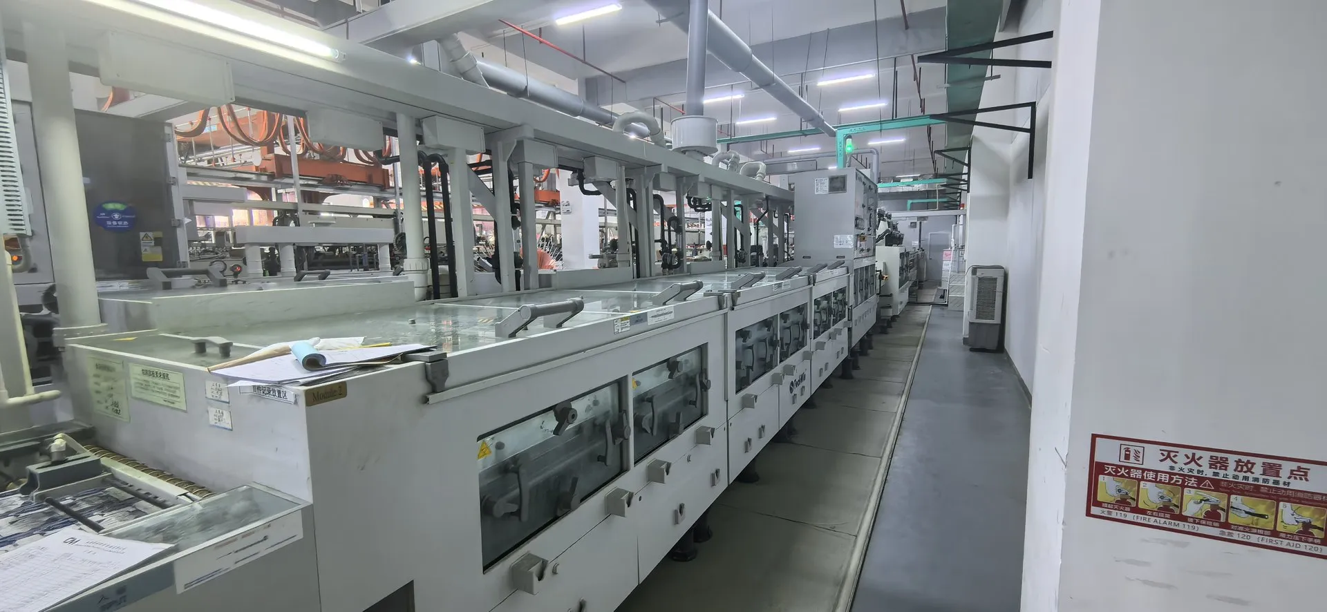

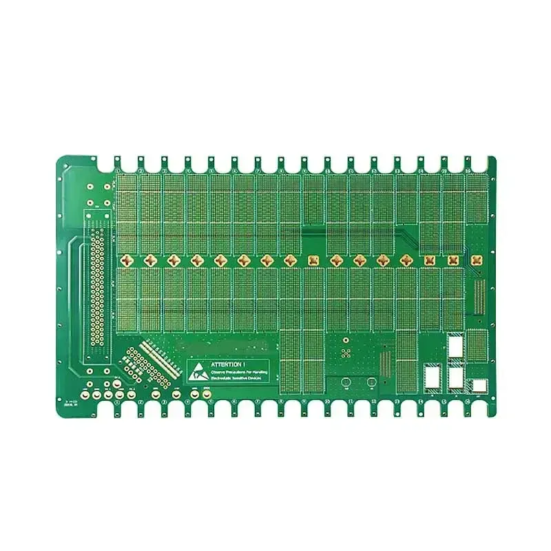
HDI technology enables higher wiring density, smaller PCB size, and improved electrical performance. However, successful HDI design is not only about using smaller vias — it requires the right balance between stackup design, via structure, and manufacturing capability.

HDI Blind & Buried Via Design Guide: Stackup & Via Filling Considerations
HDI technology enables higher wiring density, smaller PCB size, and improved electrical performance.
However, successful HDI design is not only about using smaller vias — it requires the right balance between stackup design, via structure, and manufacturing capability.
Here are key considerations engineers should keep in mind:
1. Stackup Planning
A proper HDI stackup helps ensure reliability and signal integrity.
✔ Balanced layer structure to reduce warpage
✔ Proper signal / power / ground layer arrangement
✔ Selecting suitable structures such as 1+N+1 or 2+N+2 based on requirements
2. Via Structure Selection
• Blind Via: Connects outer layers to inner layers and improves routing density.
• Buried Via: Saves surface space by connecting internal layers.
• Stacked Microvia: Enables higher density but requires stricter process control.
3. Via Filling Process
The filling method directly impacts reliability:
• Resin filling — widely used and cost-effective
• Copper filling — provides better thermal and electrical performance
• Planarization — ensures a flat surface for fine-pitch assembly
Common Design Challenges:
⚠ High aspect ratio microvias may increase filling difficulty.
⚠ Insufficient via spacing can affect reliability.
⚠ Early DFM communication is essential to avoid production issues.
HDI success comes from the combination of smart design, suitable materials, and reliable manufacturing processes.
Originally published on ShinePCB’s LinkedIn company page: 2026-07-10.
ShinePCB LinkedIn · 2026-07-10 ↗
← Engineering News