


Stack-up engineering
PCB Stack-Up Review and Layer-Specific Drill Charts
Review finished thickness, copper, reference layers and drill spans as one construction.
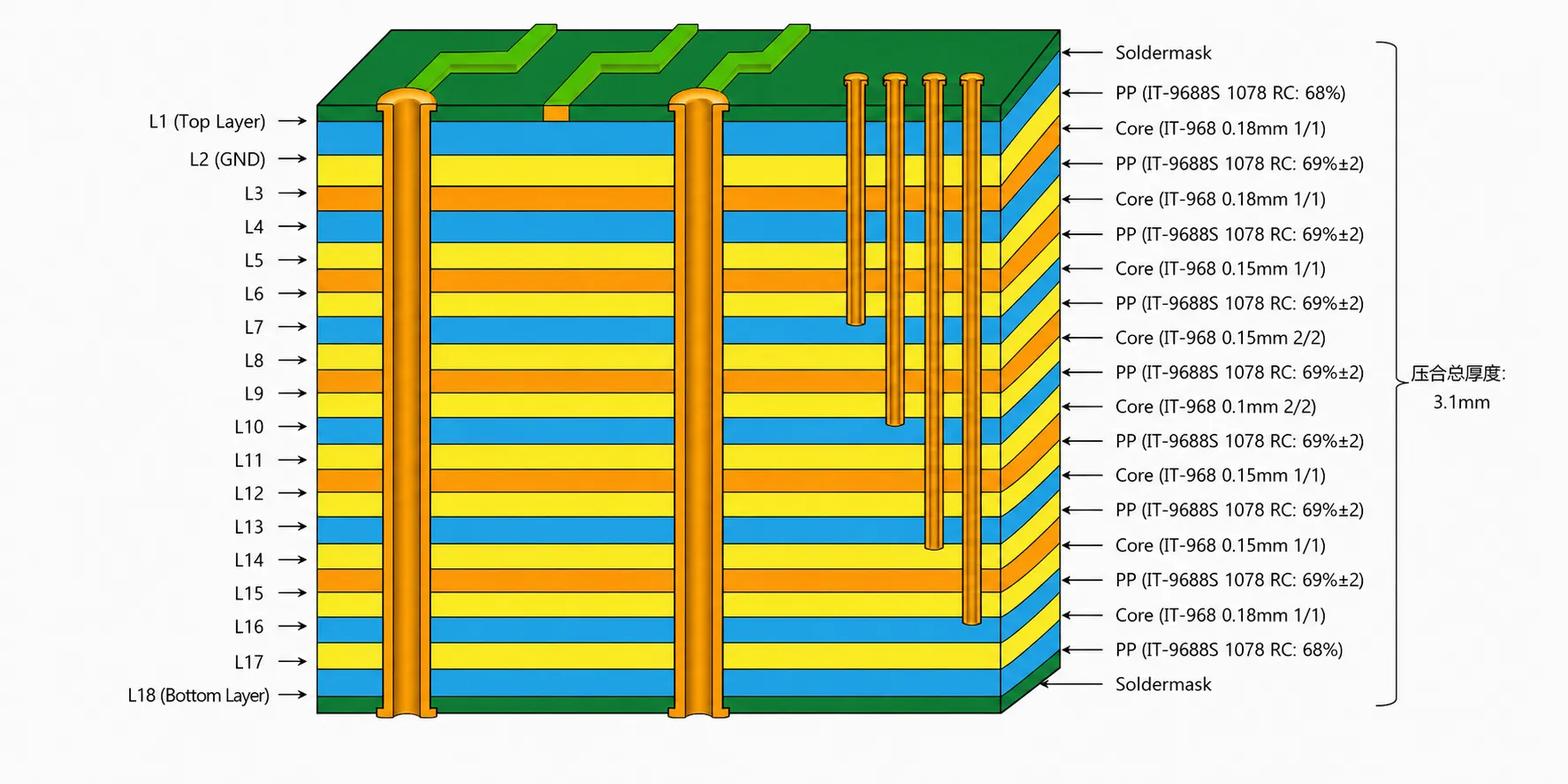
Match drill spans to their layer numbers
An archived project includes separate L1–L3 and L16–L18 drill charts. Place the start and stop layers and applicable fabrication stage next to each drill group.
Check what a material change affects
Specify the approved laminate, dielectric thickness and target impedance. If the press stack changes, revisit thickness, reference layers and the affected lines to test.
- Layer count and finished thickness
- Copper weight by layer
- Impedance targets
- Material constraints and hybrid options
Stack-up examples
Examples of PCB layer and via structures.
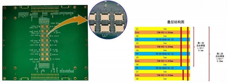
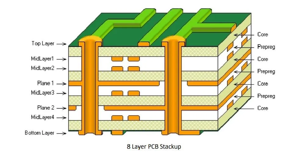
Inputs and outputs
| Inputs | Outputs |
|---|---|
| Layer count | Proposed stack-up |
| Finished thickness | Material options |
| Copper weight | Engineering questions |
| Impedance targets | Geometry proposal (with impedance engineering) |
| Material constraints | Notes on lamination cycles and cost impact |
Stack-up FAQs
Can you check my stack-up?
Yes. Send your proposed stack-up and targets for review.
Can you mix materials in one stack-up?
Hybrid stack-ups are reviewed per project. We confirm compatibility and processing before quotation.