

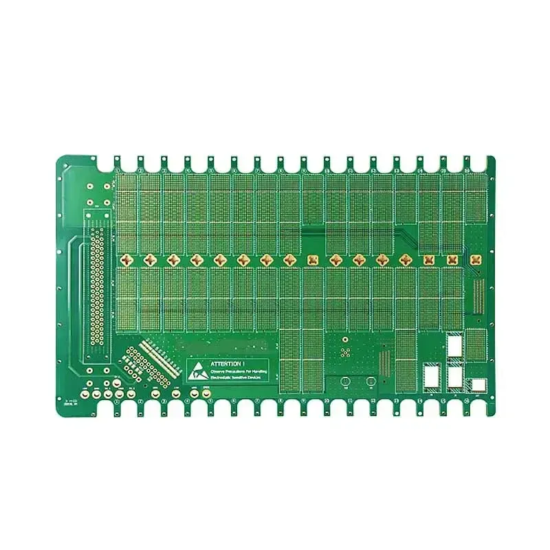
A PCB stack-up is far more than a list of copper and dielectric layers. It defines how electrical, mechanical, and thermal performance interact throughout the entire product lifecycle. Many manufacturing and field failures can be traced back to stack-up decisions made early in the design phase.…

Stack-Up Design: The Foundation of PCB Reliability
A PCB stack-up is far more than a list of copper and dielectric layers. It defines how electrical, mechanical, and thermal performance interact throughout the entire product lifecycle. Many manufacturing and field failures can be traced back to stack-up decisions made early in the design phase.
When developing a multilayer PCB, engineers should evaluate the stack-up from several perspectives:
1. Signal Integrity
Well-planned layer arrangements provide consistent reference planes, controlled impedance, and predictable return current paths. These factors help reduce reflections, crosstalk, and EMI, especially in high-speed digital applications.
2. Power Integrity
The spacing between power and ground planes directly affects plane capacitance and power distribution quality. Optimizing dielectric thickness can improve transient response and reduce power noise.
3. Mechanical Reliability
Balanced copper distribution and symmetrical layer construction minimize warpage and internal stress during lamination, reflow soldering, and long-term operation. An unbalanced stack-up can increase the risk of board deformation and reliability issues.
4. Thermal Management
Copper plane placement influences heat spreading throughout the PCB. Proper stack-up planning helps dissipate heat more efficiently, improving the reliability of power devices and temperature-sensitive components.
5. Manufacturability
An effective stack-up should align with practical manufacturing capabilities, including:
• Appropriate dielectric thickness selection
• Realistic aspect ratios for plated vias
• Compatible lamination cycles
• Material combinations that ensure dimensional stability
The stack-up should never be considered after routing is complete. Instead, it serves as the framework upon which routing, impedance control, EMI performance, and manufacturability are built.
A well-designed stack-up enables engineers to achieve not only electrical performance targets but also consistent manufacturing quality and long-term product reliability.
Discussion:
When reviewing a new PCB design, which parameter do you define first—layer count, impedance requirements, or mechanical constraints?
Originally published on ShinePCB’s LinkedIn company page: 2026-07-22.
ShinePCB LinkedIn · 2026-07-22 ↗
← Engineering News