
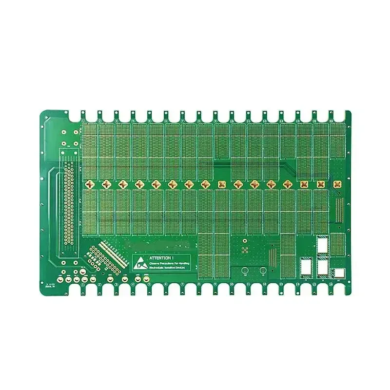
Many people see a finished PCB and only see the final product. But before a PCB becomes a physical board, it goes through a complex journey of engineering verification, material processing, and precision manufacturing.

What Happens Between Gerber Files and Finished PCBs?
Many people see a finished PCB and only see the final product.
But before a PCB becomes a physical board, it goes through a complex journey of engineering verification, material processing, and precision manufacturing.
The Gerber files are only the beginning.
Here are some critical steps behind every finished PCB:
1. Engineering Review & DFM Analysis
Before production starts, manufacturing engineers review the design data.
Trace widths, spacing, drill sizes, layer stack-up, impedance requirements, and manufacturing limitations are carefully checked to identify potential risks.
A good design must not only work electrically—it must also be manufacturable.
2. Material & Stack-Up Preparation
The PCB structure is built layer by layer.
Core materials, prepregs, copper thickness, and layer arrangements all influence electrical performance, thermal behavior, and mechanical reliability.
The right stack-up is essential for stable performance.
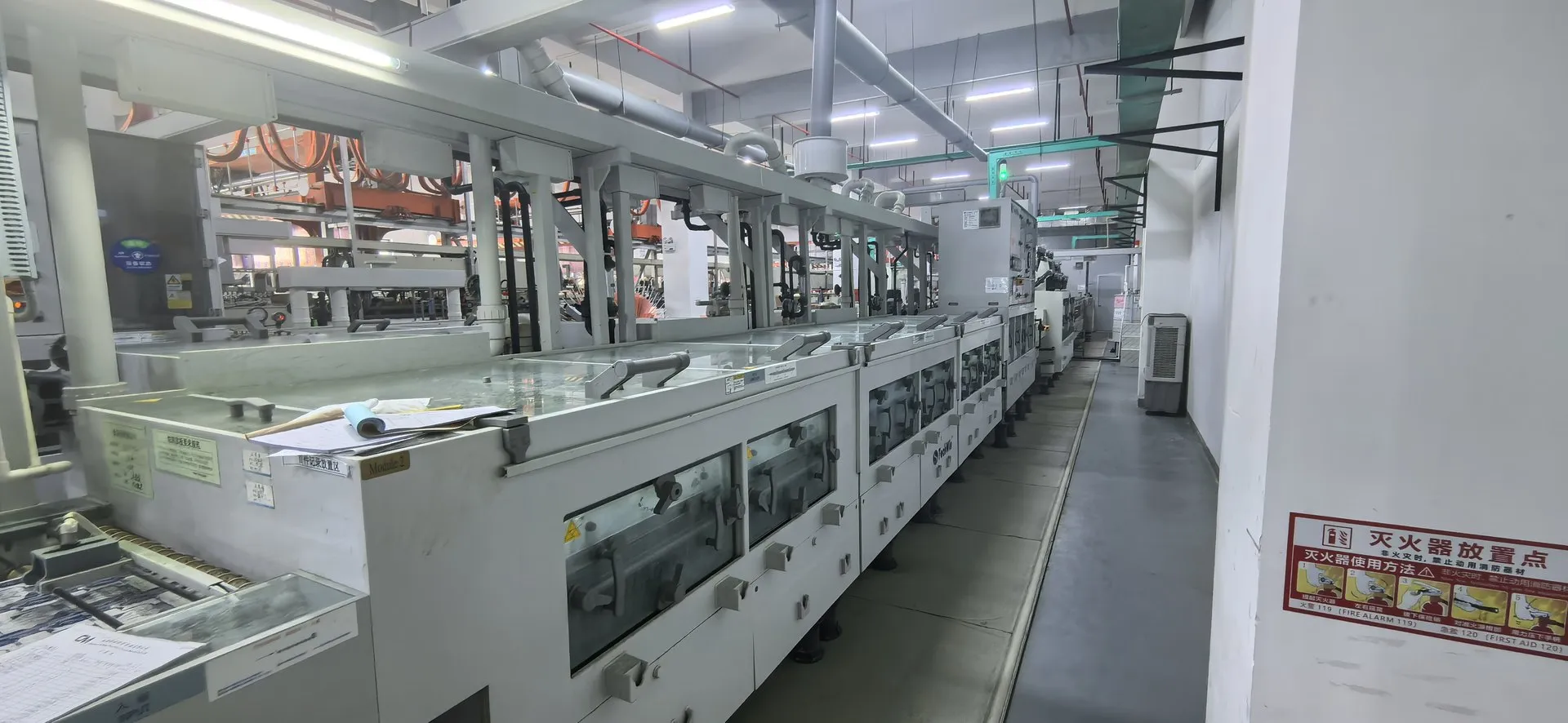
3. Imaging & Etching
The circuit patterns from the design files are transferred onto copper layers.
Advanced imaging and etching processes define the traces that will eventually carry signals and power throughout the product.
Precision at this stage directly affects circuit quality.
4. Lamination & Drilling
Multiple layers are pressed together under controlled temperature and pressure.
Then, mechanical or laser drilling creates the vias needed to connect different layers.
For HDI and high-density designs, via quality becomes especially critical.
5. Surface Finishing & Testing
Before shipment, finished boards go through surface treatment and electrical testing.
Inspection processes help verify connectivity, reliability, and compliance with design requirements.
A PCB is not simply manufactured from a file.
It is transformed through hundreds of carefully controlled steps—from digital data to a reliable electronic foundation.
Behind every successful electronic product is a manufacturing process where precision, engineering, and quality control work together.
Which stage of PCB manufacturing do you think has the biggest impact on final reliability?
Originally published on ShinePCB’s LinkedIn company page: 2026-07-30.
ShinePCB LinkedIn · 2026-07-30 ↗
← Engineering News