
When engineers discuss signal integrity, many people think about testing and debugging after a PCB is manufactured. But the reality is:

Signal Integrity Starts Long Before PCB Fabrication
When engineers discuss signal integrity, many people think about testing and debugging after a PCB is manufactured.
But the reality is:
Signal integrity is determined long before the first PCB is produced.
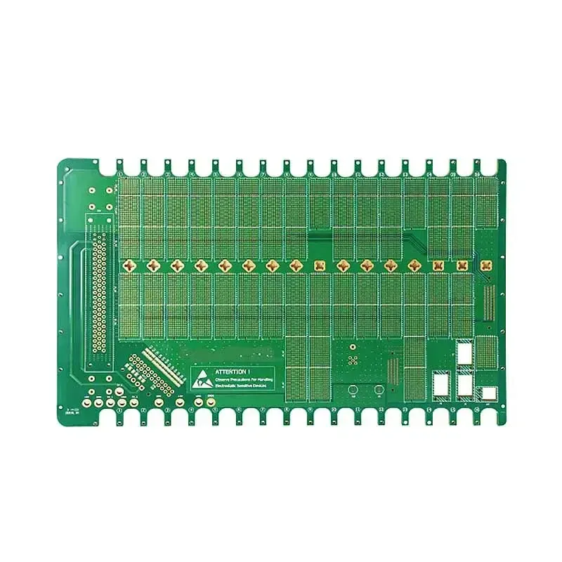
For high-speed electronic systems, every design decision can influence how signals behave in the final product.
Several key factors need to be considered from the beginning:
1. Stack-Up Design Matters
The PCB stack-up is the foundation of signal performance.
Layer arrangement, dielectric thickness, copper distribution, and reference planes directly affect impedance control and signal propagation.
A well-designed stack-up helps create predictable electrical performance.
2. Impedance Control Starts with Design
High-speed signals require controlled impedance throughout their transmission path.
Trace width, spacing, copper thickness, and material properties all work together to maintain signal quality.
Small variations can create unexpected signal loss or distortion.
3. Routing Strategy Influences Performance
PCB routing is more than simply connecting components.
Engineers need to consider:
Differential pair matching
Return current paths
Crosstalk prevention
High-speed signal layers
Good routing decisions reduce risks before manufacturing begins.
4. Material Selection Plays a Critical Role
As data rates increase, traditional materials may not always meet performance requirements.
Factors such as dielectric constant, dissipation factor, and loss characteristics become increasingly important.
5. Manufacturing Capability Supports Design Intent
Even a perfect design requires accurate manufacturing execution.
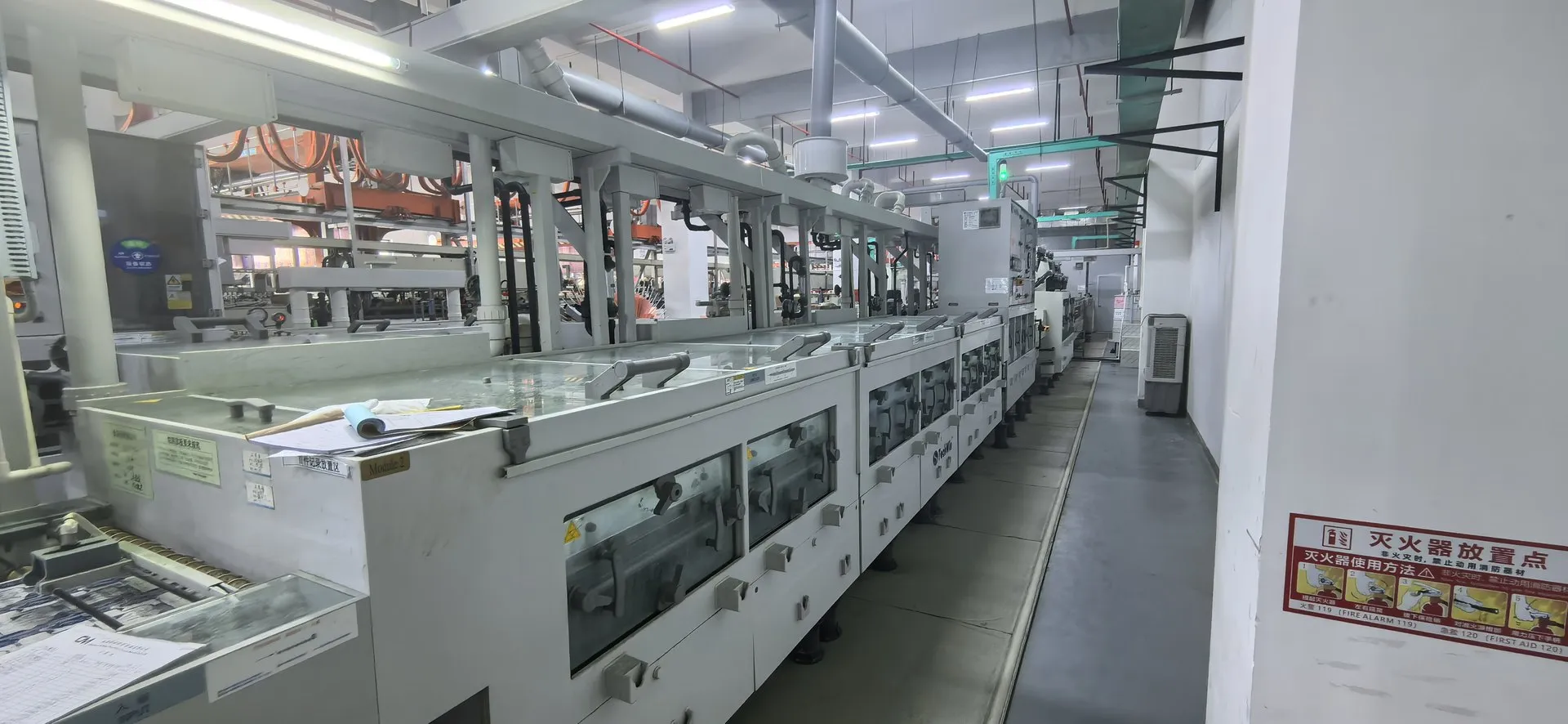
Layer alignment, copper thickness control, surface quality, and process consistency all influence whether the final PCB achieves the expected electrical performance.
Signal integrity is not created at the testing stage.
It is built step by step—from system requirements, to PCB design, to manufacturing execution.
As electronics move toward higher speeds and greater complexity, successful products depend on closer collaboration between design and manufacturing.
What do you think is the biggest challenge in high-speed PCB design: stack-up, routing, materials, or manufacturing?
Originally published on ShinePCB’s LinkedIn company page: 2026-08-10.
ShinePCB LinkedIn · 2026-08-10 ↗
← Engineering News