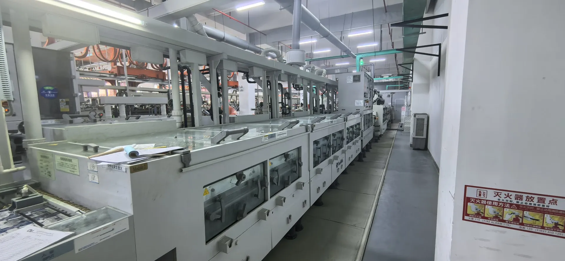

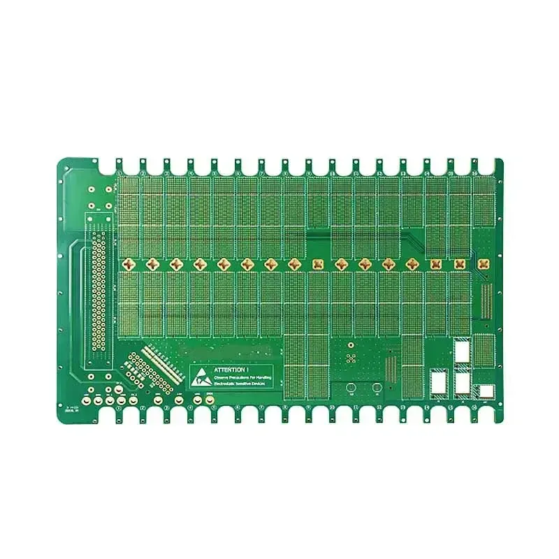
An overview of surface preparation, imaging and etching, AOI inspection, and brown oxide treatment in multilayer PCB inner-layer manufacturing.

PCB Quality Starts Long Before Final Inspection
A reliable multilayer PCB begins with precise inner-layer circuit manufacturing.
At ShinePCB, we recognize the importance of controlling every critical step in the PCB manufacturing process.
A closer look at inner-layer manufacturing:
- Surface Preparation: Cleaning and micro-etching the copper surface to improve dry-film adhesion.
- Imaging & Etching: Transferring circuit patterns and removing unwanted copper to form the designed traces.
- AOI Inspection: Using Automated Optical Inspection to identify potential defects, including open circuits, short circuits, and copper residues.
- Brown Oxide Treatment: Preparing the copper surface to improve bonding with prepreg materials during multilayer lamination.
For multilayer PCBs, quality is not determined by final inspection alone. It is built through process control at every manufacturing stage.
ShinePCB | PCB Manufacturing & PCBA Solutions
Supporting hardware development from prototyping to production.
Originally published on ShinePCB’s LinkedIn company page: 2026-10-26.
ShinePCB LinkedIn · 2026-10-26 ↗
← Engineering News